Electro-optical device, method of driving the same, and electronic apparatus using the same

a technology of electrooptical devices and electronic devices, applied in static indicating devices, instruments, photoelectric discharge tubes, etc., can solve the problems of difficult selection period and charge a pixel to a predetermined voltage, and achieve the effect of reducing power consumption

Inactive Publication Date: 2003-05-20
SEIKO EPSON CORP
View PDF1 Cites 26 Cited by
  • Summary
  • Abstract
  • Description
  • Claims
  • Application Information

AI Technical Summary

Benefits of technology

is to provide an electro-optical device capable of reducing the power consumption and charging each pixel sufficiently within the selection period, as well as a driving method of such an electro-optical device and an electronic apparatus using such an electro-optical device.

Problems solved by technology

This results in a problem that charging a pixel to a predetermined voltage in the selection period becomes more difficult as the distance between the source of the data signal voltages such as a data line driving circuit and the pixel to be charged becomes longer or the screen size of the liquid crystal device becomes larger.

Method used


Image

  • Electro-optical device, method of driving the same, and electronic apparatus using the same
  • Electro-optical device, method of driving the same, and electronic apparatus using the same
  • Electro-optical device, method of driving the same, and electronic apparatus using the same

Examples


first embodiment

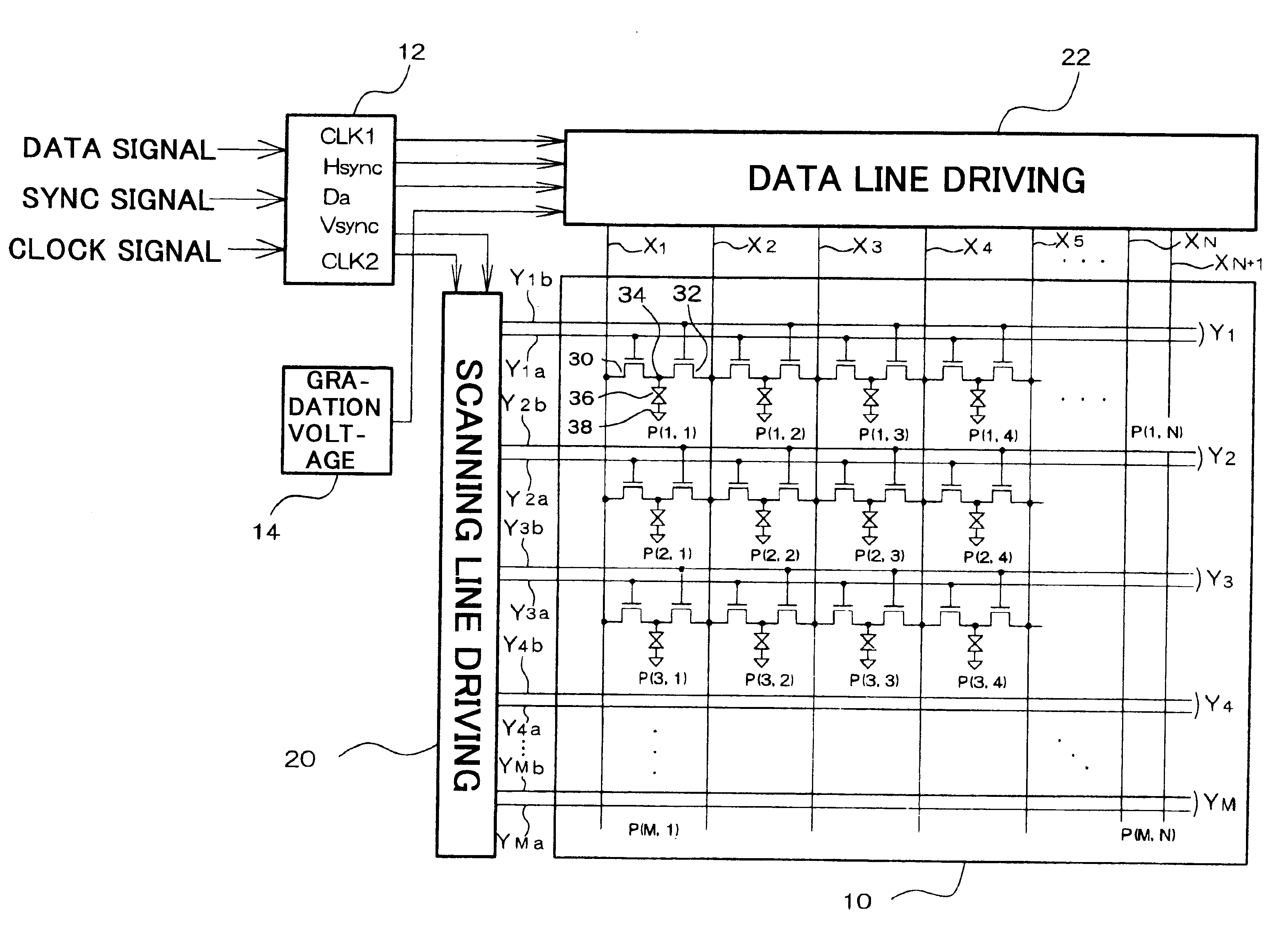
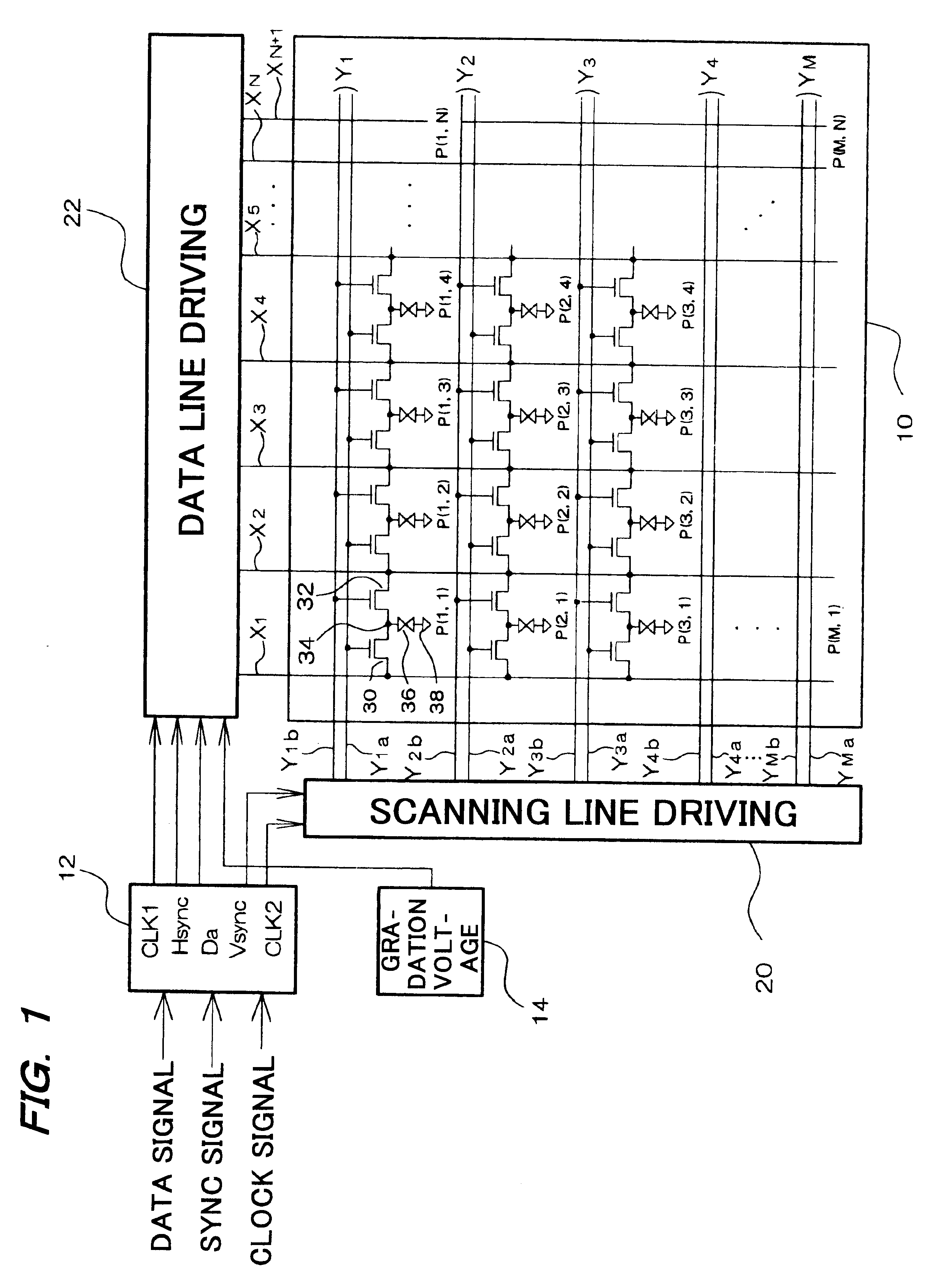
FIG. 1 shows a TFT liquid crystal device according to a first embodiment of the invention.

The liquid crystal device is composed of a liquid crystal panel 10, a signal control circuit section 12, a gradation voltage circuit section 14, a scanning line driving circuit 20, and a data line driving circuit 22. In FIG. 1, the individual pixels of the liquid crystal panel 10 are denoted by P (1, 1), . . . , P (m, n), . . . P (M, N), where m, n, M, and N are integers that are greater than or equal to 2.

Reference characters Y and X generically denote scanning lines and data lines, respectively, and symbols Y.sub.1, Y.sub.2, . . . , Y.sub.M and X.sub.1, X.sub.2, . . . , X.sub.N, X.sub.N+1 denote individual scanning lines and data lines, respectively. Moreover, Y.sub.1a, Y.sub.1b, Y.sub.2a, Y.sub.2b, . . . , Y.sub.Ma, Y.sub.Mb denote further specific scanning lines.

The scanning lines Y.sub.1 to Y.sub.M and the data lines X.sub.1 to X.sub.N+1 are arranged in the liquid crystal panel 10 and the ...

second embodiment

FIG. 9 is a block diagram showing a TFT liquid crystal device according to a second embodiment of the invention. The liquid crystal device having this configuration provides the same advantages as the liquid crystal device according to the first embodiment does.

This liquid crystal device is composed of a liquid crystal panel 110, a signal control circuit section 112, a gradation voltage circuit section 114, a scanning line driving circuit 120, and a data line driving circuit 122. In FIG. 9, the individual pixels of the liquid crystal panel 110 are denoted by P (1, 1), . . . , P (M, N). Reference characters Y and X generically denote scanning lines and data lines, respectively, and symbols Y.sub.1, Y.sub.2, . . . , Y.sub.M and X.sub.1, X.sub.2, . . . , X.sub.N denote specific scanning lines and data lines. Moreover, Y.sub.1a, Y.sub.1b, Y.sub.2a, Y.sub.2b, . . . , Y.sub.Ma, Y.sub.Mb denote further specific scanning lines, and X.sub.1a, X.sub.1b, X.sub.2a, X.sub.2b, . . . , X.sub.Na, X...


PUM

PropertyMeasurementUnit
voltageaaaaaaaaaa
voltage amplitudeaaaaaaaaaa
polarityaaaaaaaaaa

Abstract

A liquid crystal panel has odd-numbered data lines Xa to which a positive data signal voltage is supplied and even-numbered data lines Xb to which a negative data signal voltage is supplied. The liquid crystal panel has MxN pixels P (m, n) that are arranged in such a manner that each pixel P(m, n) corresponds to one of the odd-numbered data lines and one of the even-numbered data lines that is adjacent to the one odd-numbered data line. The aperture portion of each pixel P (m, n) is provided with a switching element that is connected to a scanning line Ym and one of the data lines Xa, and a switching element that is connected to the scanning line Ym and one of the data lines Xb that is adjacent to the one data line Xa. In performing dot inversion driving on this liquid crystal device, a data line driving circuit supplies positive data signal voltages to the data lines Xa and negative data signal voltages to the data lines Xb. In synchronism with this operation, a scanning line driving circuit controls opening / closing of the two switching elements.

Description

Japanese Patent Application No. 2000-209564, filed Jul. 11, 2000, is hereby incorporated by reference in its entirety.1. Field of the InventionThe present invention relates to an electro-optical device, a method of driving the electro-optical device, and an electronic apparatus using the electro-optical device.2. Description of Related ArtAt present, in TFT (thin-film transistor) liquid crystal devices, for example, AC voltage driving methods such as frame inversion driving, line inversion driving, and dot inversion driving are used. Among those driving methods, the dot inversion driving method is a driving method capable of preventing flicker and a luminance gradient. As shown in FIG. 12A, the dot inversion driving method is such that the phase is inverted on a pixel-by-pixel basis. The operation of a liquid crystal device using the dot inversion method will be described below by using one particular pixel P(1, 1) as an example.FIG. 12B shows how the voltage V.sub.P(1, 1) of the pi...

Claims


Application Information

Patent Timeline
Patent Type & Authority Patents(United States)
IPC IPC(8): G09G3/36G02F1/133G09G3/20
CPCG09G3/3688G09G2310/0297G09G2310/027
Inventor MORITA, AKIRA
Owner SEIKO EPSON CORP
Why Eureka
Try Eureka