
Eureka
For R&D, Eureka makes reading and utilizing patents & technical documents easy.
Eureka AIR
Designed for self-driven R&D workflows. Generate viable solutions, solve complex R&D challenges, empower your innovation with AI.

Eureka Materials
Designed for material experts only. Revolutionize your material R&D, from search, analyze, to developing new materials.

TechResearch
Generate reliable direction feasibility study reports for your R&D in just a few steps.

TechSeek
Discover and master advanced knowledge NOW. Basics, ideas, possibilities, all at once.

TechMind
As an expert in R&D Theories, TechMind can generates customized viable solutions instantly.

TechRisk
Analyze your overall solution with one click, know your potential R&D risks in advance.

TechMonitor
Get weekly tech updates, stay abreast of the latest tech innovations and key insights.
Semiconductor device
- Summary
- Abstract
- Description
- Claims
- Application Information
AI Technical Summary
Problems solved by technology
Method used
Image

Examples
embodiment 1
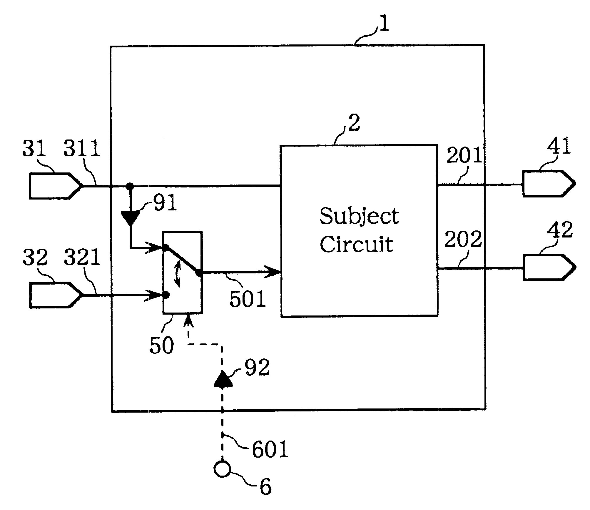
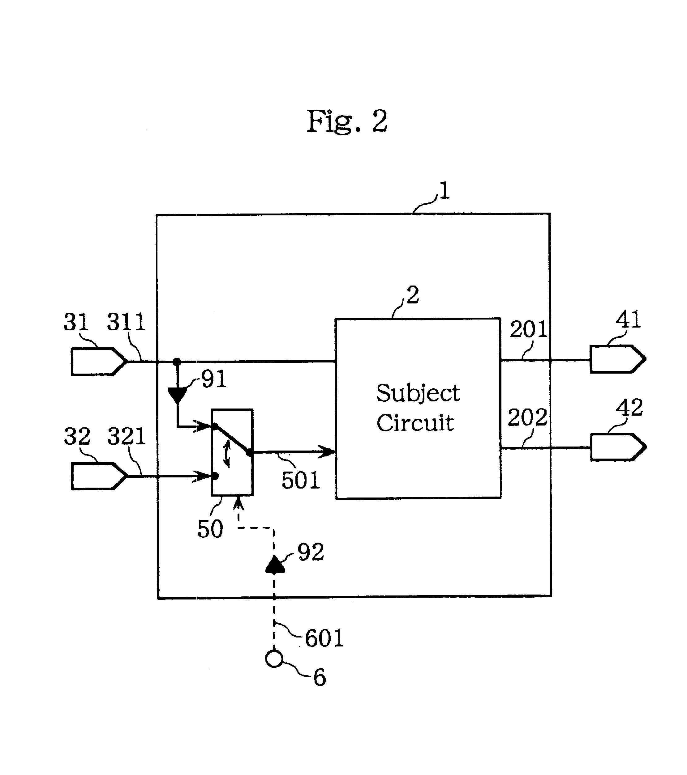
FIG. 2 shows a configuration of a semiconductor device according to It is noted here that in FIGS. 1 and 2, like reference numerals refer to like parts, and their respective descriptions are not repeated here. In addition, for the sake of brevity and clarity in figures, scan chains in the subject circuit 2 are not shown in the drawings. It is also noted that like reference numerals designate like parts throughout the accompanying drawings.
The semiconductor device 1 of FIG. 2 mainly differs from the foregoing prior-art device in that the device 1 of FIG. 2 comprises 1) a selector 50 provided between a second input terminal 32 to which a burn-in data is not supplied and a second scan chain which corresponds to the second input terminal 32, 2) a selecting signal input terminal 6 provided for feeding a selecting signal 601 to the selector 50, and 3) an amplifying circuit 91. The amplifying circuit 91 can be eliminated if the driving performance of the input signal is sufficient.
In the ...
embodiment 2
This embodiment is a variation of the foregoing Embodiment 1, in which plural selectors are provided in parallel.
FIGS. 3A and 3B show configurations of a semiconductor device according to this embodiment. As shown in FIG. 3A, a plurality of scan chains are connected to the subject circuit 2 to be burned-in in the semiconductor device 1. In FIG. 3A, the reference numerals 33 and 34 denote a third and fourth input terminals respectively, and the reference numerals 43 and 44 a third and fourth output terminals respectively. The reference numeral 51 denotes a first selector, the reference numeral 52 a second selector, the reference numeral 53 a third selector. Each of the reference numerals 61, 62, and 63 denotes a selecting signal input terminal of the respective selectors, and each of the reference numerals 611, 621, and 631 denotes a selecting signal fed from each respective selecting signal input terminal to each of the selectors. The reference numeral 91 denotes an amplifying circu...
embodiment 3
This embodiment is a variation of the foregoing Embodiment 2, in which a plurality of the selectors are connected in cascade as shown in FIG. 4A.
FIGS. 4A and 4B show configurations according to this embodiment. In a semiconductor device as shown in FIGS. 4A and 4B, it is made possible that a burn-in data from a single input terminal can be simultaneously supplied to a plurality of scan chains, as well as in a semiconductor device according to Embodiment 2.
FIGS. 4A and 4B respectively correspond to FIGS. 3A and 3B. FIG. 4A illustrates a semiconductor device 1 in which selecting signal input terminals 61, 62, and 63 are respectively provided for selectors 51, 52, and 53, and FIG. 4B illustrates a semiconductor device 1 having a control signal input terminal 60 and a control circuit 7.
According to this embodiment, since the selectors are connected in cascade as shown in FIG. 4A, it becomes unnecessary to consider a fan out (driving performance) of an input signal to be supplied to many...
PUM
 Abstract
Description
Claims
Application Information
 - R&D Engineer
- R&D Manager
- IP Professional
- Industry Leading Data Capabilities
- Powerful AI technology
- Patent DNA Extraction
Browse by: Latest US Patents, China's latest patents, Technical Efficacy Thesaurus, Application Domain, Technology Topic, Popular Technical Reports.
© 2024 PatSnap. All rights reserved.Legal|Privacy policy|Modern Slavery Act Transparency Statement|Sitemap|About US| Contact US: help@patsnap.com