

Apparatus and method for embedded boundary scan testing
a technology of boundary scan and embedded circuit, which is applied in the direction of detecting faulty computer hardware, error detection/correction, instruments, etc., can solve the problems of inability to conduct boundary scan testing, the testing of pcbs and the implemented electrical circuits of pcbs is often complex, and the board testing at manufacture has become increasingly automated, so as to facilitate the testing of ieee 1149.1, enhance the test coverage
- Summary
- Abstract
- Description
- Claims
- Application Information
AI Technical Summary
Benefits of technology
Problems solved by technology
Method used
Image

Examples
Embodiment Construction
[0019]Referring now to the figures, several embodiments or implementations of the various aspects of the present disclosure are hereinafter illustrated and described in conjunction with the drawings, wherein like reference numerals are used to refer to like elements.
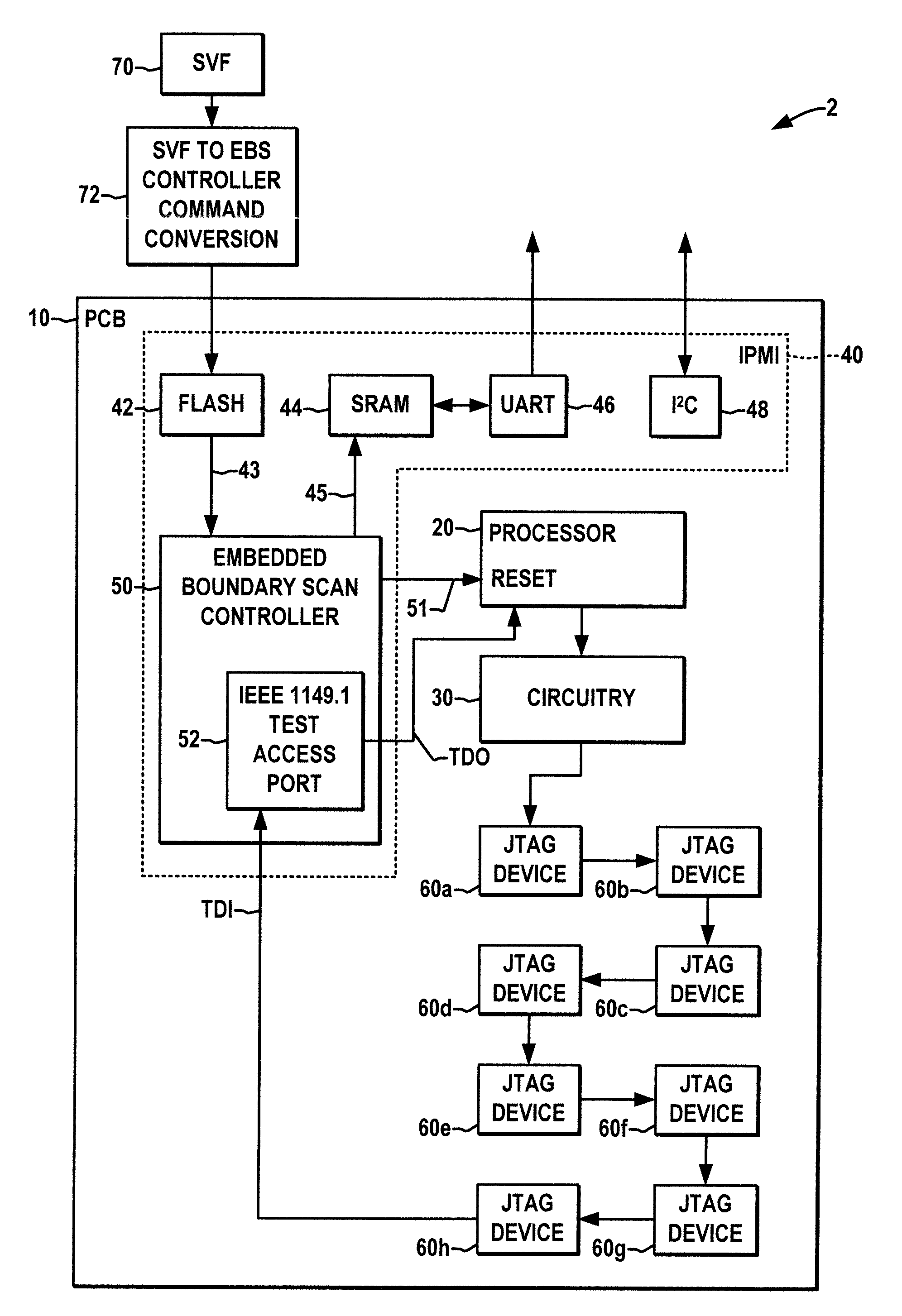
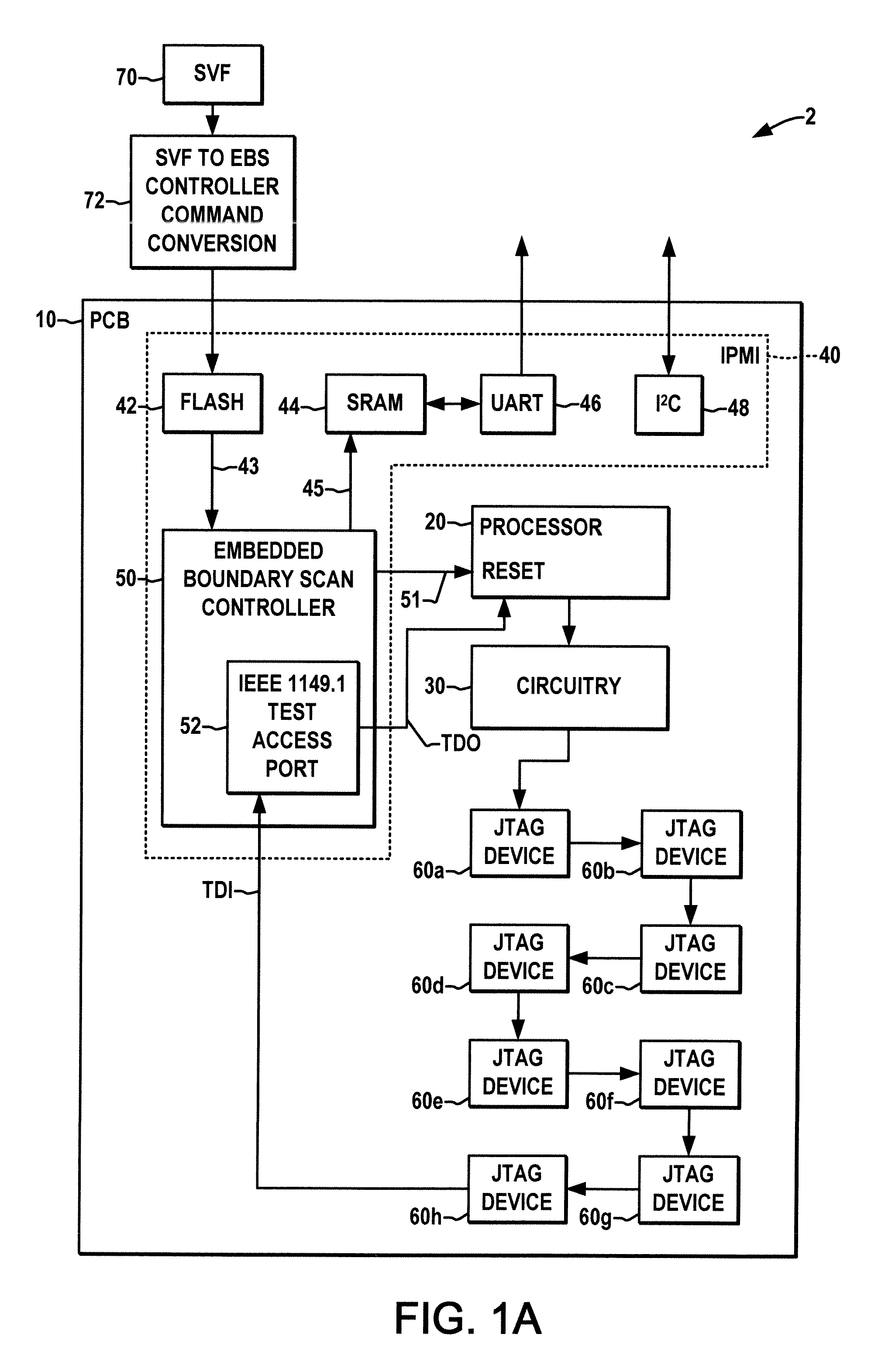
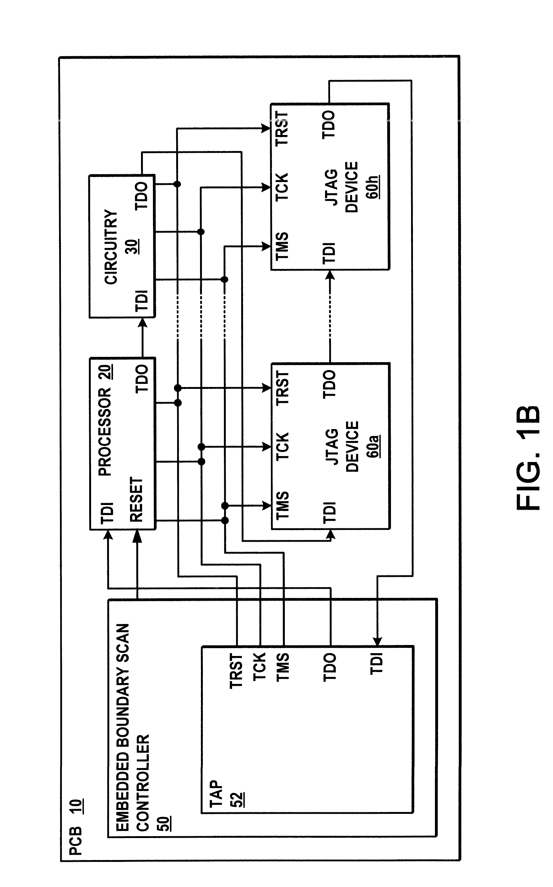
[0020]FIGS. 1A-1C illustrate an exemplary PCB apparatus 10 with a processor system 20 and an embedded boundary scan testing system 40 in accordance with various aspects of the present disclosure, where FIG. 1A shows an initial situation 2 in which boundary scan commands and vectors are stored into an on-board non-volatile memory, such as when the board 10 is manufactured. The PCB 10 can be any type of processor-based circuit board, for example, an LCP2, LCP3, or LCP6 6U CompactPCI® (cPCI) and CompactPCI® Packet Switched Backplane (cPSB) card 10 for use in a platform feature server telecommunications system application in the illustrated embodiments. In one implementation shown in FIG. 1A, the boundary scan system is inco...
PUM
 Abstract
Description
Claims
Application Information