Manufacturing method of a gate-split flash memory

a manufacturing method and technology of gate-split flash memory, applied in the direction of basic electric elements, electrical apparatus, semiconductor devices, etc., can solve the problems of incompatibility of the gate-split flash memory process with the modern gate-split flash memory process, poor removal rate, and uneven gate lengths

Inactive Publication Date: 2003-07-08
WINBOND ELECTRONICS CORP
View PDF4 Cites 35 Cited by
  • Summary
  • Abstract
  • Description
  • Claims
  • Application Information

AI Technical Summary

Problems solved by technology

A disadvantage of the STI technology is incompatible with the process of the modern gate-split flash memory.
A prior art method which increases a barrier oxide layer to generate a self-aligned salicide floating memory will cause unequal gate lengths and bad removal rate.
Generally speaking, if a misalignment happens in defining the floating gate by a pattern of a mask, the channel length and operational characteristic of the flash memory will be heavily affected.
However, only below the control gate, the peak can develop the function of field emission, and peaks on the other places not only fail to develop the function of field emission, but also affect an yield of the salicide process.
In conclusion, the peaks only beneath the control gate have the ability of erasing data stored in the flash memory, and peaks on the other positions do not have the ability and lead to a short circuit, current leakage or being salicided, because they are exposed outside the control gate after a spacer etching is executed.
In this circumstance, if the contacts inside the flash memory are etched, the channel length between the source region and floating gate will be shortened and an error will happen.

Method used


Image

  • Manufacturing method of a gate-split flash memory
  • Manufacturing method of a gate-split flash memory
  • Manufacturing method of a gate-split flash memory

Examples


Embodiment Construction

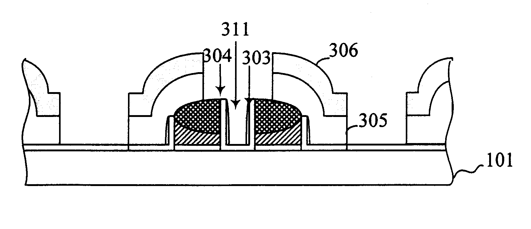
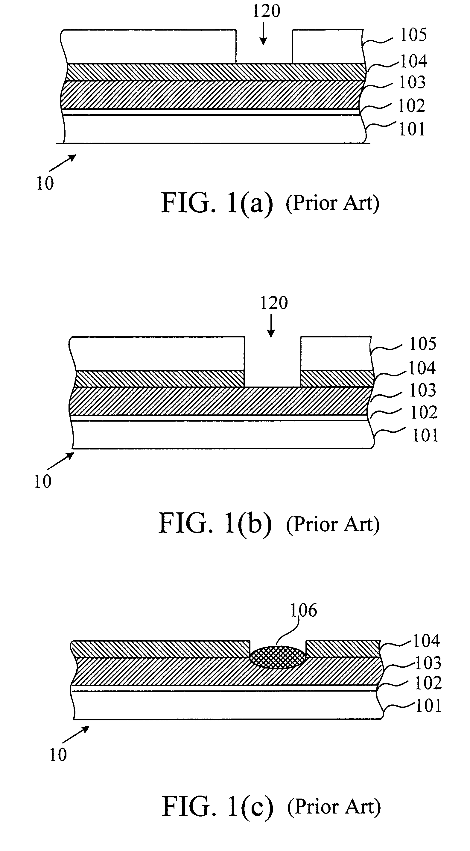
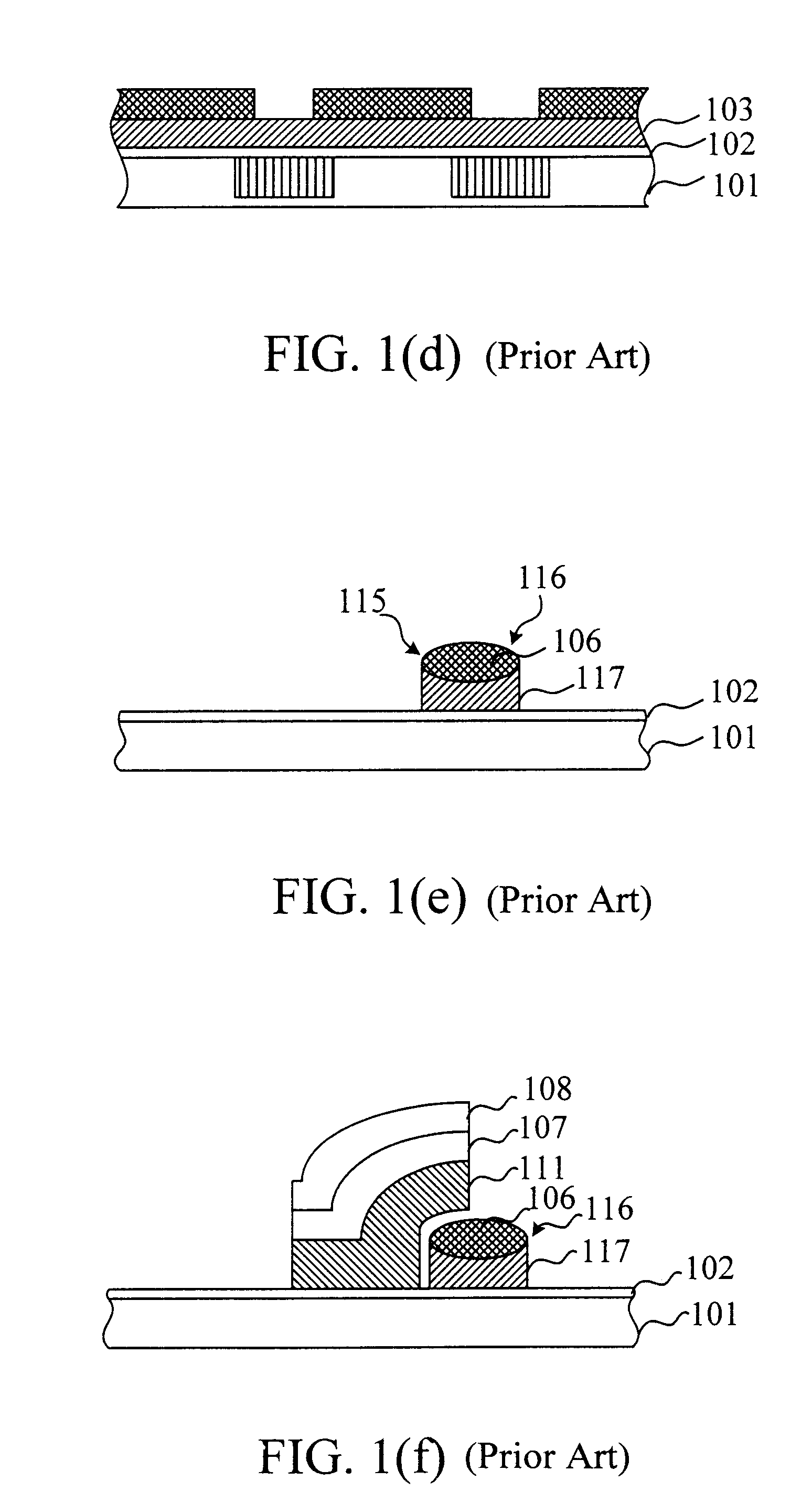
FIGS. 3(a).about.(i) show a manufacturing flow of a flash memory using a self-align contact process according to the present invention. In FIG. 3(a), a flash memory 30 comprises a substrate (such as P carrier) 101, a tunnel dielectric layer 102, a first polysilicon layer 103 acting as a floating gate region, a first hard material layer (such as a silicon nitride Si.sub.3 N.sub.4) 104 and a channel mask 105. The channel mask 105 has an opening 120 for forming a floating gate region. In FIG. 3(b), the silicon nitride layer 104 corresponding to the opening region 120 is etched, thermally forming a polysilicon-oxide region 106. The cross section of the polysilicon-oxide region 106 appears like an ellipse in FIG. 3(b), and on its both sides, a bird's beak effect is induced. In FIG. 3(c), spacer nitrides 301 are deposited on the intersection of the polysilicon-oxide region 106 and the silicon nitride layer 104, and the deposition lengths of both regions are the same. In FIG. 3(d), the pol...


PUM


Abstract

The present invention relates to discloses a manufacturing method of a gate-split flash memory, which is suitable for a self-align contact process and fully-salicide-compatible process. The present invention masks the invalid peaks with a thick passivation layer to obtain the purpose of removing the invalid peaks in the manufacturing process of a gate-split flash memory. The present invention deposits a nitride spacer to define a pattern of a floating gate of the flash memory, so that a channel length of the floating gate can be finely defined. The present invention also utilizes a mask pattern to define the floating gate region of the flash memory, and the manufacturing process will be smooth and cheap.

Description

1. Field of the InventionThe present invention relates to a manufacturing method of a gate-split flash memory, and particularly to a manufacturing method of a gate-split flash memory which can remove unnecessary peaks in a floating gate polysilicon region.2. Description of Related ArtFor a prior art manufacturing method of a flash memory, a source region of the flash memory is manufactured by a similar resist-stripping way. Therefore, if there is a demand to reduce the size of the flash memory, a STI technology is always used, which separates the source region into several parts and connecting them by a plurality of local wires. A disadvantage of the STI technology is incompatible with the process of the modern gate-split flash memory. A prior art method which increases a barrier oxide layer to generate a self-aligned salicide floating memory will cause unequal gate lengths and bad removal rate. Generally speaking, if a misalignment happens in defining the floating gate by a pattern...

Claims


Application Information

Patent Timeline
Patent Type & Authority Patents(United States)
IPC IPC(8): H01L21/70H01L27/115H01L21/8247H01L29/40H01L29/423H01L21/28H01L21/336
CPCH01L21/28273H01L27/115H01L27/11521H01L29/42324H01L29/66825H01L29/40114H10B69/00H10B41/30
Inventor HUANG, SHUI-CHIN
Owner WINBOND ELECTRONICS CORP
Why Eureka
Try Eureka