Bidirectional signal control circuit

a control circuit and bidirectional signal technology, applied in logic circuit coupling/interface arrangement, pulse technique, instruments, etc., can solve the problems of rc wiring delay rapidly increasing, long wiring length, and difficulty in activating the semiconductor integrated circuit at high speed

Inactive Publication Date: 2003-10-14
LAPIS SEMICON CO LTD
View PDF4 Cites 5 Cited by
  • Summary
  • Abstract
  • Description
  • Claims
  • Application Information

AI Technical Summary

Problems solved by technology

However, with recent advances in scale down of a semiconductor integrated circuit, a delay due to load capacity and resistance, which results from a wiring length, becomes predominant.
This RC wiring delay rapidly increases as compared with a gate delay.
Thus, the transfer of bidirectional signals under the configuration shown in FIG. 2 has created difficulties in activating the semiconductor integrated circuit at high speed.
Therefore, a delay of each output control signal on the signal line for supplying the output control signal could lead to a hindrance to speeding up even if the speeding up of the transfer of each signal to the wire would be implemented.
Thus, a problem arises in that a further speeding-up is difficult.

Method used


Image

  • Bidirectional signal control circuit
  • Bidirectional signal control circuit
  • Bidirectional signal control circuit

Examples


Embodiment Construction

A preferred embodiment of the present invention will hereinafter be described with reference to the accompanying drawings.

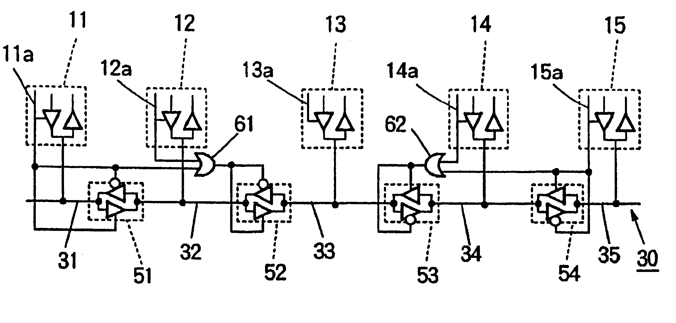
FIG. 1 is a circuit diagram showing a configuration of a two-way or bidirectional signal control circuit according to an embodiment of the present invention. Upon description of the present embodiment, the same elements of structure as those employed in the bidirectional signal control circuit shown in FIG. 3 are identified by the same reference numerals.

Referring to FIG. 1, reference numeral 30 indicates a wire or interconnection used for two-way or bidirectional signals. Reference numerals 51, 52, 53 and 54 indicate bidirectional buffers placed in the course of the wire 30 respectively. The wire 30 is divided into five wiring parts or sections 31, 32, 33, 34 and 35 by the bidirectional buffers 51 through 54.

Further, reference numerals 11, 12, 13, 14 and 15 indicate tri state drivers placed at output lines electrically connected to their corresponding wiring sec...


PUM


Abstract

A wire used for transferring bidirectional signals is divided into a plurality of sub line segments. These sub line segments are classified into groups. Further, bidirectional buffers are provided between respective adjacent sub wires. The direction of transfer of a signal by each of the bidirectional buffers is controlled based on at least one of control signals used to control drivers for respectively outputting data signals to the sub line segments.</PTEXT>

Description

1. Field of the InventionThe present invention relates to a bidirectional signal control circuit, and particularly to a bidirectional signal control circuit for controlling the transfer of data signals outputted from a plurality of tri state drivers through a wire used for bidirectional signals.2. Description of the Related ArtUpon the design of an LSI, a plurality of functional blocks are placed over one chip and an interconnection or wire is used to connect between the functional blocks. It is common that designed blocks registered in a library are placed and a wire for transferring unidirectional or bidirectional signals is used to connect between the blocks. Such a semiconductor integrated circuit needs a high-speed operation. Therefore, it is also necessary to contrive the wire.FIG. 2 is a diagram showing connections for transferring bidirectional signals, which are employed in a conventional semiconductor integrated circuit.In FIG. 2, reference numeral 10 indicates an intercon...

Claims


Application Information

Patent Timeline
Patent Type & Authority Patents(United States)
IPC IPC(8): H03K19/173H03K19/0175H03K19/003G06F3/00
CPCH03K19/00323H03K19/1736H03K19/01759
Inventor NAKATA, MITSUNORI
Owner LAPIS SEMICON CO LTD
Why Eureka
Try Eureka