Layout method for bit line sense amplifier driver

a technology of amplifier driver and sense amplifier, which is applied in the field of sense amplifier and sense amplifier driver, can solve problems such as noise when the bit line sense amplifier senses data

Inactive Publication Date: 2003-12-09
SAMSUNG ELECTRONICS CO LTD
View PDF6 Cites 18 Cited by
  • Summary
  • Abstract
  • Description
  • Claims
  • Application Information

AI Technical Summary

Problems solved by technology

Further, since the contact MC6 is connected to the active region of the first driver N5, which has a large area, due to an increase in junction loading, noise occurs when the bit line sense amplifier senses data.

Method used


Image

  • Layout method for bit line sense amplifier driver
  • Layout method for bit line sense amplifier driver
  • Layout method for bit line sense amplifier driver

Examples


Embodiment Construction

The present invention will be described more fully hereinafter with reference to the accompanying drawings in which a preferred embodiment of the invention is shown. Like reference numerals refer to like elements throughout the drawings.

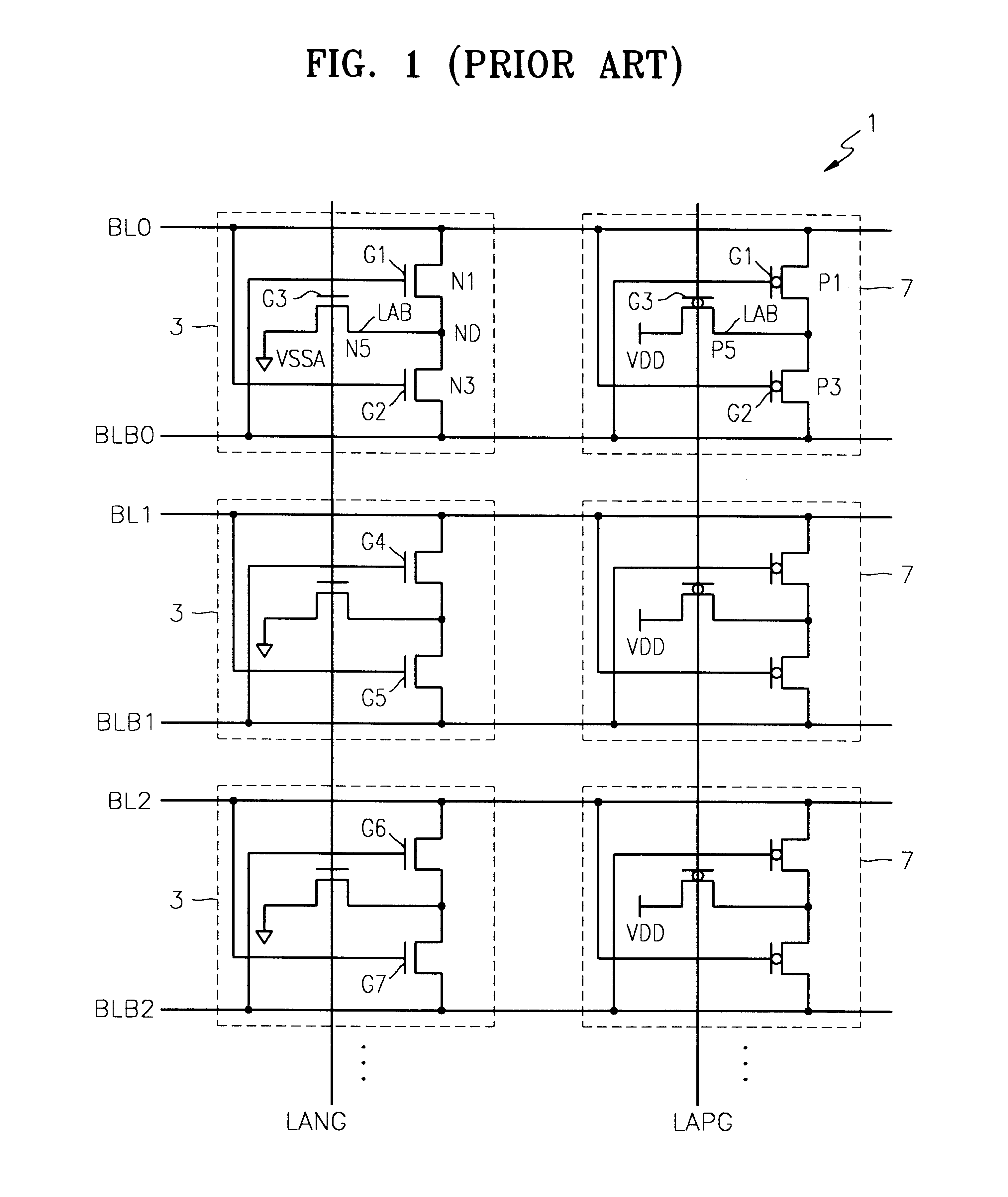
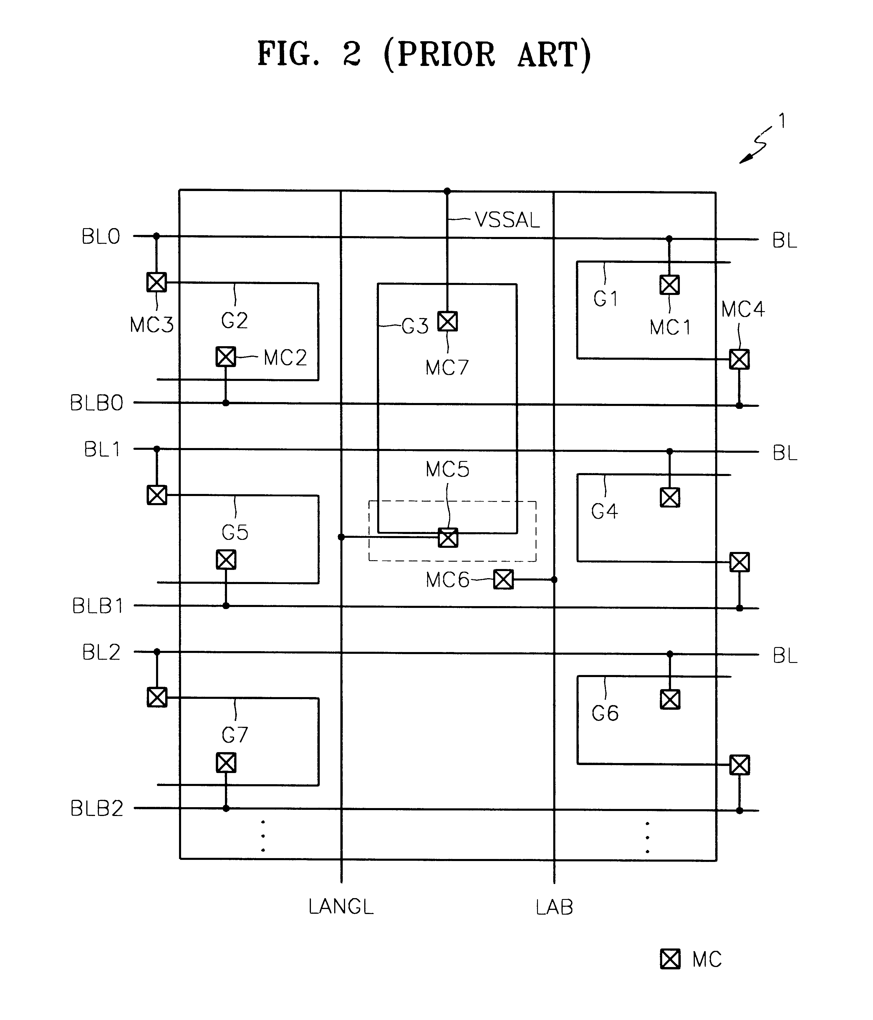
In general, a semiconductor memory device includes a plurality of memory cell arrays in which a plurality of memory cells are arranged in a matrix configuration, a bit line sense amplifier for sensing data stored in the memory cells between the memory cell arrays, and drivers for supplying a predetermined voltage to the bit line sense amplifier.

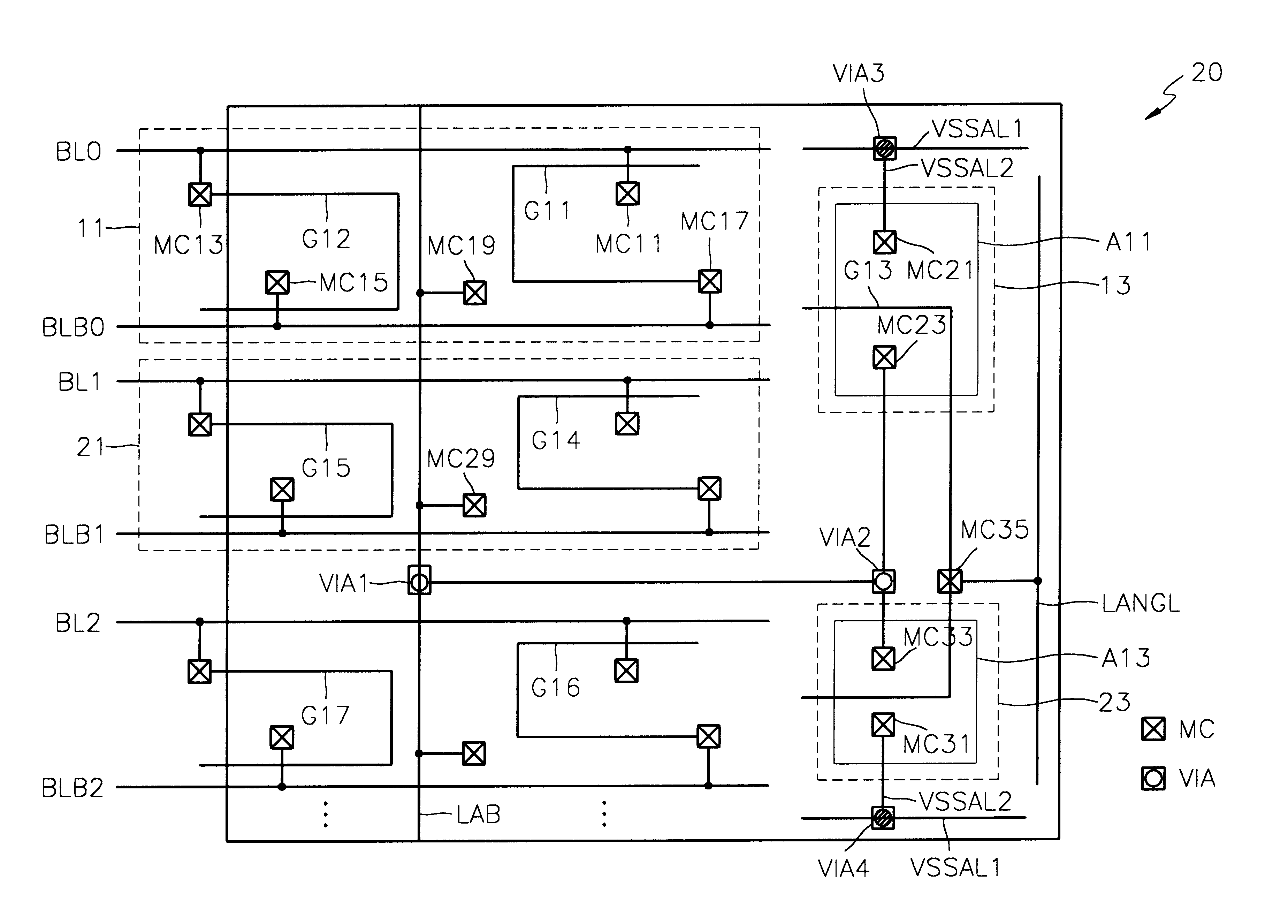
FIG. 3 is a circuit diagram of a bit line sense amplifier according to a preferred embodiment of the present invention. Referring to FIG. 3, a bit line sense amplifier 10 includes a first sense amplifier block 20 and a second sense amplifier block 30. Preferably, the first and second sense amplifier blocks 20 and 30 are laid out symmetrically.

The first sense amplifier block 20 includes a plurality of NMOS sens...


PUM


Abstract

A bit line sense amplifier is provided. The bit line sense amplifier includes a first sense amplifier block in which a plurality of first sense amplifiers for sensing and amplifying data of a bit line or a complementary bit line are laid out, and first drivers, which are arranged outside the plurality of first sense amplifiers, for pulling down the bit line or the complementary bit line to a first voltage level. The bit line sense amplifier further includes a second sense amplifier block with a plurality of second sense amplifiers and second drivers for pulling up the bit line or the complementary bit line to a second voltage level. By arranging the drivers outside the bit sense amplifiers, effects caused by variation in critical dimensions (CDs) of gates are minimized and the entire area of the bit line sense amplifier is reduced.

Description

PRIORITYThis application claims priority to an application entitled "LAYOUT METHOD FOR BIT LINE SENSE AMPLIFIER DRIVER" filed in the Korean Industrial Property Office on Jul. 20, 2001 and assigned Serial No. 2001-43790, the contents of which are hereby incorporated by reference.1. Field of the InventionThe present invention relates to semiconductor circuits, and more particularly, to a layout method for a sense amplifier and a sense amplifier driver.2. Description of the Related ArtIn general, a bit line sense amplifier senses, amplifies, and outputs data of a memory cell selected by an address.FIG. 1 is a circuit diagram of a conventional bit line sense amplifier. Referring to FIG. 1, a bit line sense amplifier 1 used in a DRAM includes a plurality of NMOS sense amplifiers 3 and a plurality of PMOS sense amplifiers 7 that are arranged symmetrically for maximization of characteristics. Hereinafter, for the convenience of explanation, one NMOS sense amplifier 3 and one PMOS sense amp...

Claims


Application Information

Patent Timeline
Patent Type & Authority Patents(United States)
IPC IPC(8): G11C7/06H01L27/02H01L21/8242G11C7/08G11C11/401G11C11/409H01L27/108
CPCH01L27/0207G11C7/065G11C7/06
Inventor LEE, JAE-YOUNGCHOI, JONG-HYUN
Owner SAMSUNG ELECTRONICS CO LTD
Why Eureka
Try Eureka