Light emitting device including an electroconductive layer

an electroconductive layer and light-emitting device technology, applied in the field of optoelectric elements, can solve problems such as the difficulty of applying the luminescent layer onto the optoelectri

Inactive Publication Date: 2004-02-03
LUMILEDS
View PDF18 Cites 54 Cited by
  • Summary
  • Abstract
  • Description
  • Claims
  • Application Information

AI Technical Summary

Problems solved by technology

The problem is, however, that it is often difficult to apply the luminescent layer onto the optoelectric element in such a manner that a closely contacting layer of a readily controlled and substantially uniform thickness is obtained.

Method used


Image

  • Light emitting device including an electroconductive layer
  • Light emitting device including an electroconductive layer

Examples


Embodiment Construction

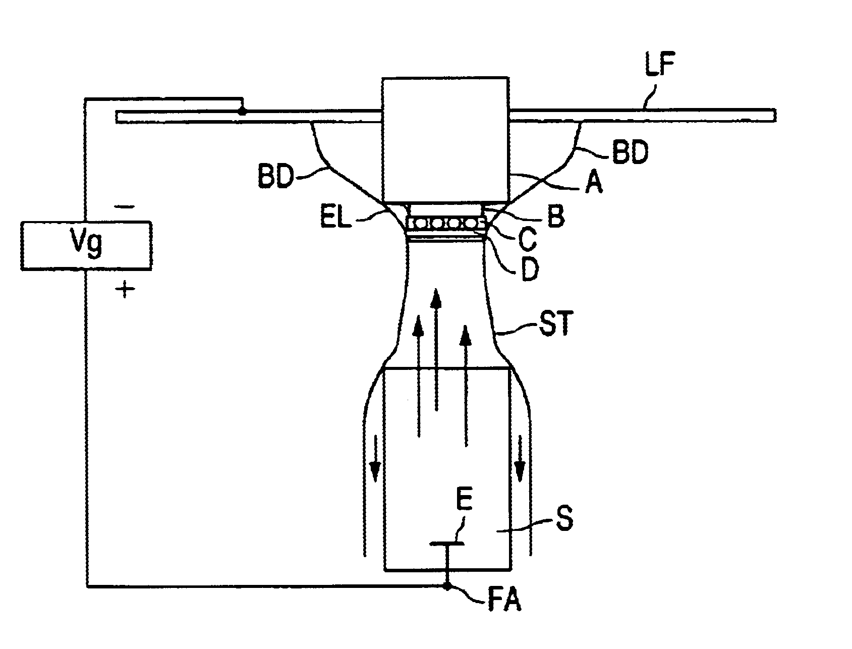
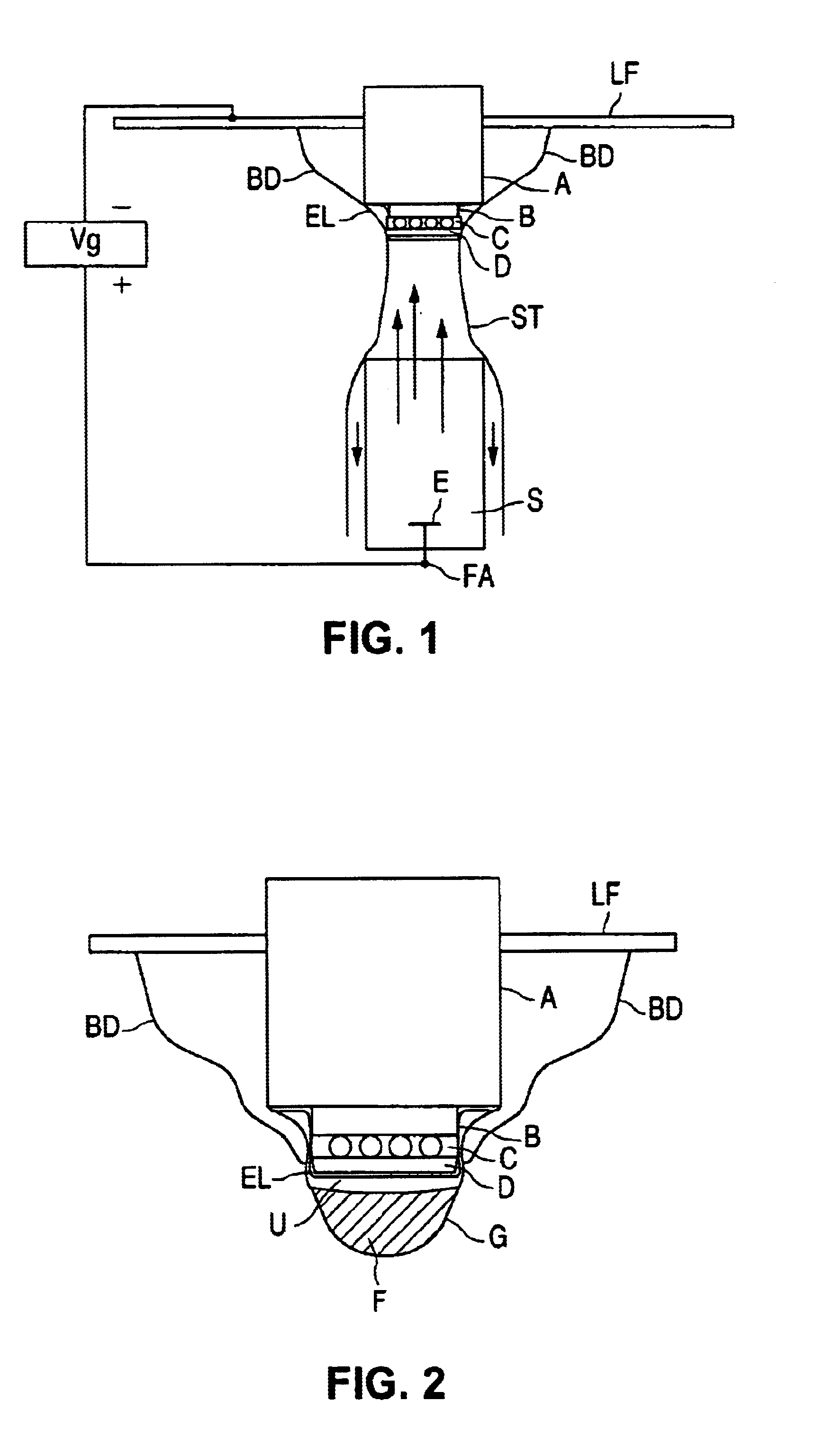
In FIG. 1, LF denotes a carrier plate of an electroconductive material. A denotes a heat sink, which is provided in a hole in the carrier plate LF and which is made from a metal. On the heat sink A there is provided a submount B composed of a Si wafer covered with a layer of aluminum. Ends of the submount B are connected to respective bonding wires, which are each connected to the carrier plate LF. D denotes a LED, which comprises a substrate made from an electrically insulating ceramic material on which a number of epitaxial layers consisting of a semiconductor material are provided. These epitaxial layers jointly form a semiconductor body. C denotes solder balls forming electric contacts between LED D and submount B. ST denotes a droplet of a suspension S of a luminescent material. The droplet ST is in contact with a part of the outside surface of heat sink A, submount B, contacts C and LED D. The part of the outside surface of heat sink A, submount B, contacts C and LED D contact...


PUM

PropertyMeasurementUnit
thicknessaaaaaaaaaa
electric conductivityaaaaaaaaaa
electroconductiveaaaaaaaaaa

Abstract

A LED is covered with an electroconductive layer, and a luminescent layer is deposited on the electroconductive layer by electrophoresis. The conductivity of the electroconductive layer is chosen to be such that the layer can be used as one of the electrodes during the electrophoresis, while the LED is not short-circuited by the electroconductive layer during normal operation.

Description

1. Field of the InventionThe invention relates to an optoelectric element having a semiconductor body provided on a substrate formed from an electrically insulating material and covered with a luminescent layer for converting electromagnetic radiation of a first wavelength range generated by the semiconductor body into visible light of a different wavelength range.The invention also relates to a method of covering an optoelectric element with a luminescent layer.2. Description of the Related ArtA prior art optoelectronic element as just mentioned is disclosed in U.S. Pat. No. 5,813,752. In the known optoelectric element, the semiconductor body and the substrate form part of a LED. The luminescent layer converts UV light or blue light generated by the LED into visible light of a different wavelength range. In this manner, such LEDs can be made suitable for use in different applications requiring visible light of different colors. The problem is, however, that it is often difficult to...

Claims


Application Information

Patent Timeline
Patent Type & Authority Patents(United States)
IPC IPC(8): H01L33/00C09K11/02H01L33/50
CPCH01L33/507H01L2924/0002H01L2924/00
Inventor VERHOECKX, GODEFRIDUS JOHANNESVAN LETH, NICOLAAS JOSEPH MARTINVISSER, CORNELIS GERARDUS
Owner LUMILEDS
Why Eureka
Try Eureka