

Three-dimensional photonic crystal waveguide apparatus
a waveguide apparatus and three-dimensional technology, applied in the field of three-dimensional photonic crystal waveguide apparatus, can solve the problem of not being able to guide light in paths which extend in three dimensions
- Summary
- Abstract
- Description
- Claims
- Application Information
AI Technical Summary
Benefits of technology
Problems solved by technology
Method used
Image

Examples
Embodiment Construction
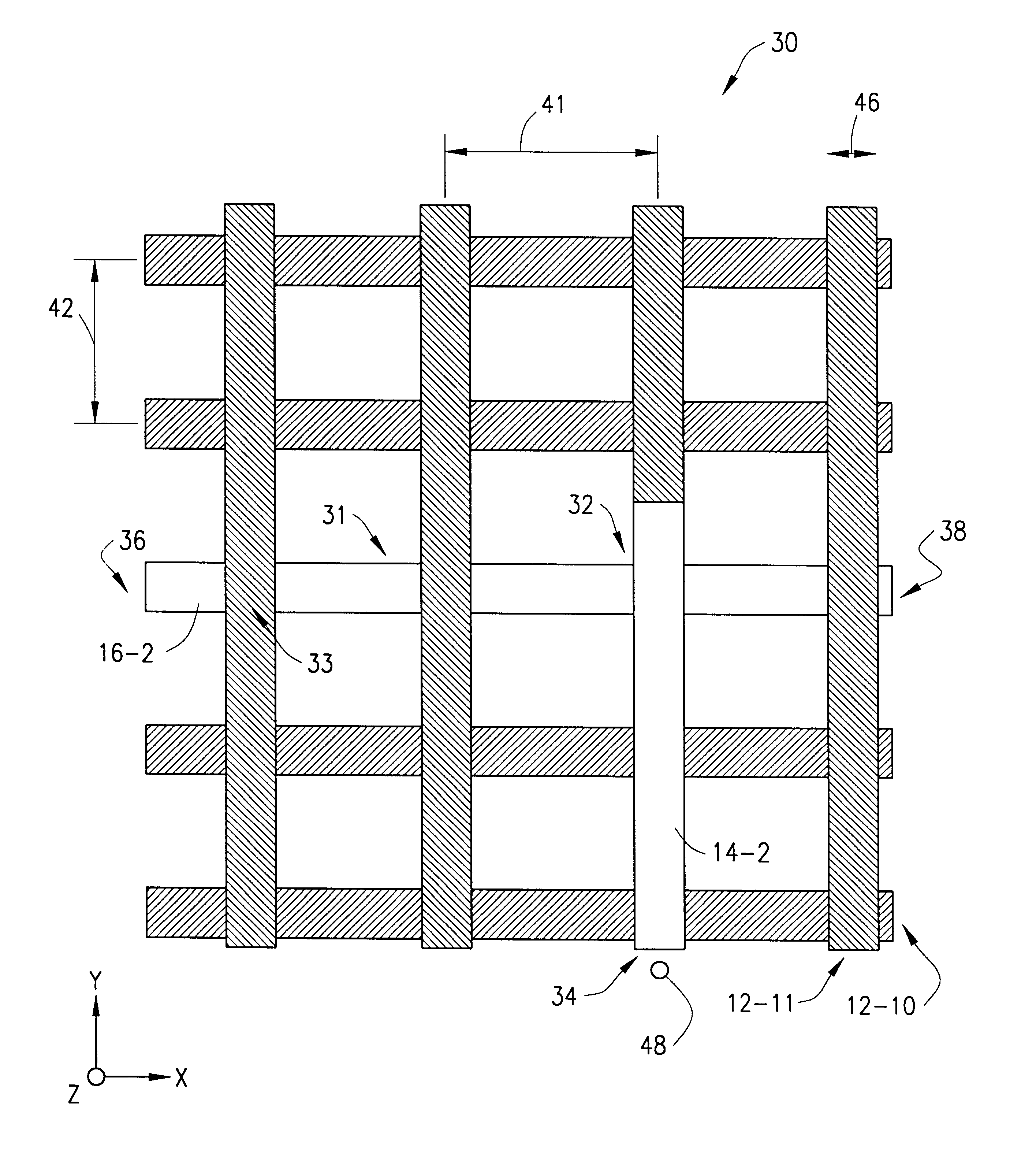
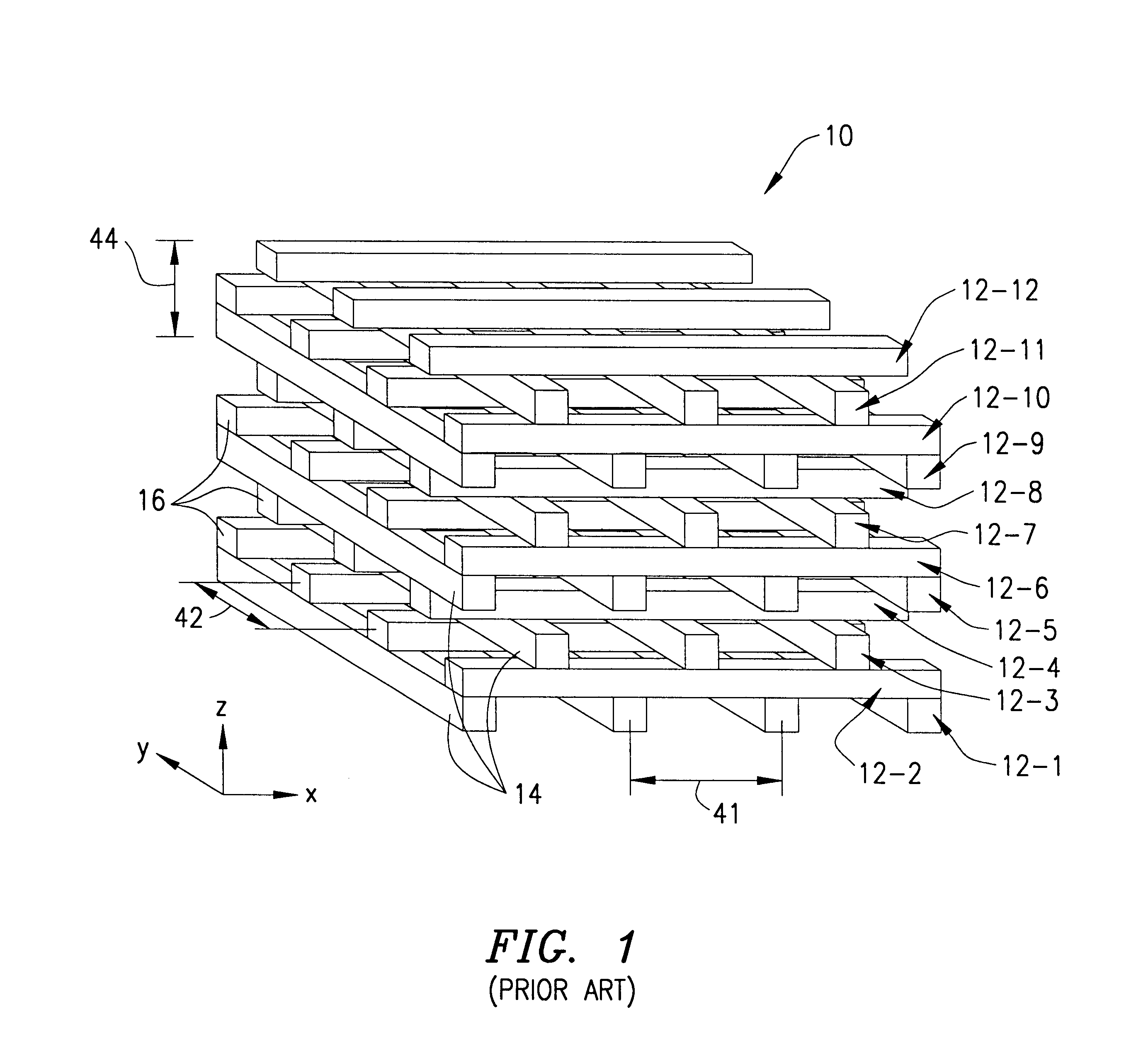
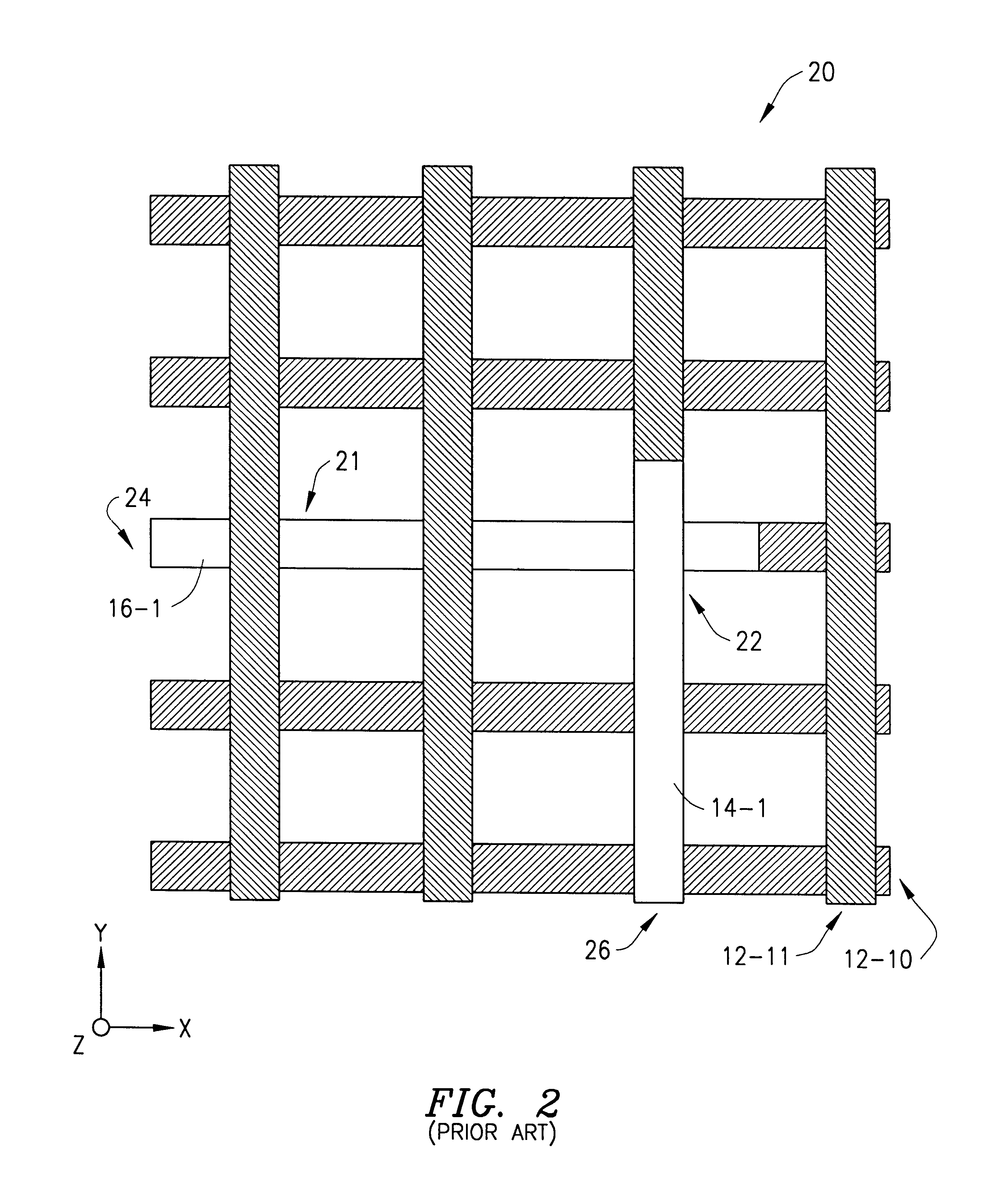
Three-dimensional photonic crystal waveguide apparatus are known in the art. In particular, FIG. 1 is a schematic, perspective view of a known three-dimensional photonic crystal apparatus (see K. M. Ho, et al., Solid State Commun., 89,413,1994 and U.S. Pat. Nos. 5,335,240 and 5,406,573) that may include an optical waveguide therein, and that is described herein to assist in explaining the present invention. The apparatus is generally designated by reference number 10 and comprises a three-dimensional photonic crystal composed of a plurality a layers arranged one on top of another. In FIG. 1, three-dimensional photonic crystal apparatus 10 comprises twelve layers 12-1 to 12-12. although the apparatus can comprise any desired plurality of layers.
Each layer 12-1 to 12-12 comprises a plurality of elements arranged to be parallel to and equally spaced from one another. In addition, the plurality of elements in each layer are arranged perpendicular to the elements in an adjacent layer.
In ...
PUM
 Abstract
Description
Claims
Application Information