
Using a model specific register as a base I/O address register for embedded I/O registers in a processor

Inactive Publication Date: 2004-03-23
GLOBALFOUNDRIES INC
View PDF14 Cites 30 Cited by
  • Summary
  • Abstract
  • Description
  • Claims
  • Application Information

AI Technical Summary

Problems solved by technology

However, the use of MSRs may be undesirable because such use may lead to nonstandard solutions across different processor models.
In addition, access to such registers is restricted to software having a certain privilege level.
Thus, access to MSR registers through RDMSR and WRMSR instructions are limited to software operating at CPU Privilege Level=0, also referred to as ring 0.
However, that solution would undesirably increase processor pin count and / or potentially modify an industry standard processor pin configuration.

Method used


Image

  • Using a model specific register as a base I/O address register for embedded I/O registers in a processor
  • Using a model specific register as a base I/O address register for embedded I/O registers in a processor
  • Using a model specific register as a base I/O address register for embedded I/O registers in a processor

Examples


Embodiment Construction

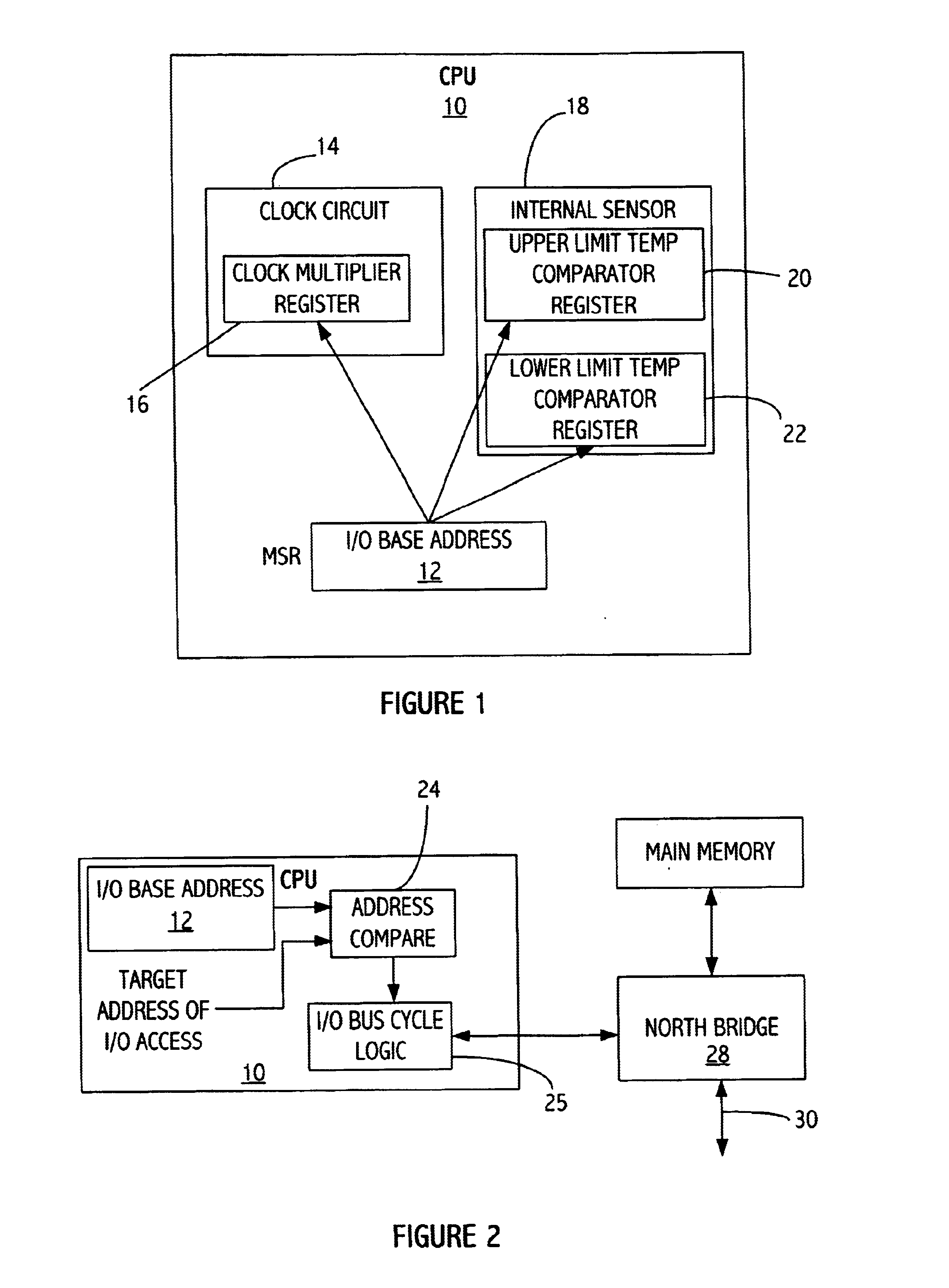
FIG. 1 illustrates a microprocessor 10 incorporating features of the present invention that allows embedded functions to be located on microprocessor 10 and be accessed as I / O ports in I / O address space. MSR register 12 functions as a base address register which is loaded with an appropriate base address during, e.g., system start-up by BIOS code. That base address is mapped into I / O address space. Various exemplary embedded functions are illustrated on CPU 10. For example, CPU 10 may include clock control circuit 14, which includes clock multiplier register 16. That register specifies the multiplication factor for a received bus clock (not shown) to determine a clock frequency for microprocessor core logic.

FIG. 1 illustrates another exemplary embedded function, temperature sensor 18, that may be incorporated into a microprocessor. Illustrated along with temperature sensor 18 are two registers 20 and 22 which set the upper and lower limit for comparing the temperature detected by th...


PUM


Abstract

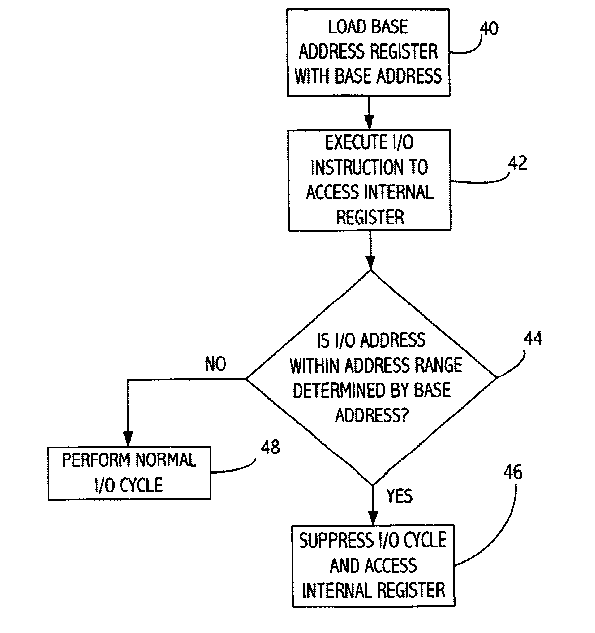
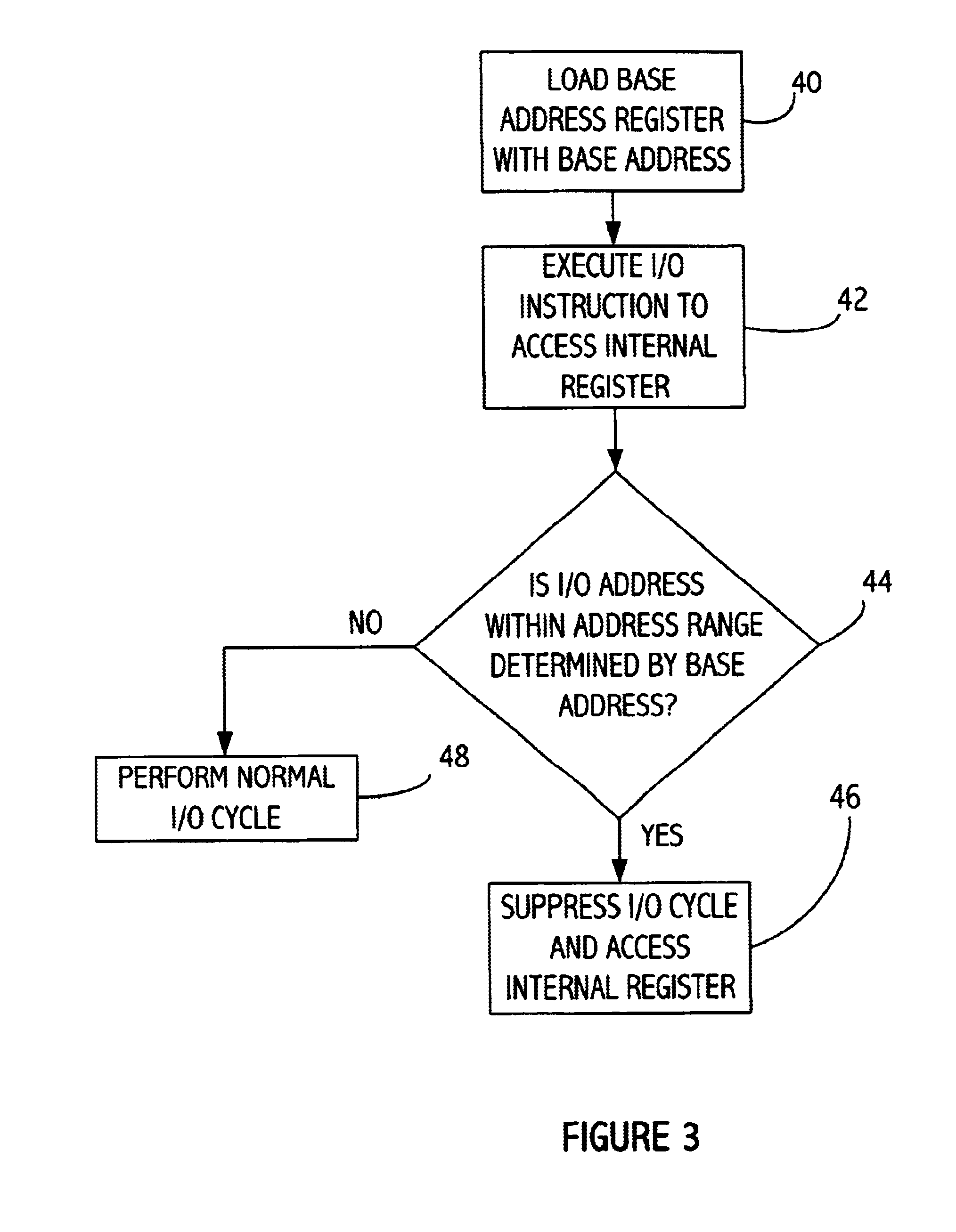
A processor includes an input / output (I / O) register that is mapped into input / output (I / O) address space. The processor also includes a base address register that is loaded with a base address. The base address register may be a model specific register (MSR). The input / output register is accessed with an input / output instruction at an address determined according to the base address and an offset therefrom. The base address register may be accessible to software operating at a high privilege level and not accessible to software operating at a lower privilege level, while the I / O register is accessible to software operating at the lower privilege level. The processor determines when an I / O access is to the processor I / O register and accesses that I / O register without causing an input / output bus cycle that would otherwise occur.

Description

1. Field of the InventionThe invention relates to microprocessors and more particularly to accessing registers on a microprocessor, which are mapped into input / output memory space.2. Description of the Related ArtIn traditional x86 architectures, the processor has both memory and input / output (I / O) mapped address space. With I / O mapped I / O, registers of peripheral devices are accessed through I / O instructions, which access the registers (also referred to herein as ports) in I / O address space. A signal line (M / IO) indicates to logic external to the processor whether the processor is addressing an I / O mapped I / O port during execution of an I / O instruction or whether the processor is accessing memory (or a memory-mapped I / O port) as a result of an instruction fetch or an instruction that loads or stores data.As levels of integration continue to increase in processors, additional I / O like functions are expected to be added to processors. It is possible that the functions could be access...

Claims


Application Information

Patent Timeline
IPC IPC(8): G06F12/14G06F9/30G06F9/312G06F9/318G06F9/355
CPCG06F9/30043G06F9/30101G06F9/30181G06F9/342G06F12/1491
Inventor MITCHELL, CHARLES WELDONQURESHI, QADEER AHMADCALDWELL, DERVINN DEYUAL
Owner GLOBALFOUNDRIES INC
Learn More