Circuit board capable of protecting an MR magnetic head therein against electrostatic breakdown and magnetic head using the same

a circuit board and mr magnetic head technology, applied in the field of circuit boards, can solve the problems of mr magnetic head device 208 suffering electrostatic breakdown, clip may slip off, and increase the production cost of the magnetic head

Inactive Publication Date: 2004-05-04
TDK CORPARATION
View PDF4 Cites 6 Cited by
  • Summary
  • Abstract
  • Description
  • Claims
  • Application Information

AI Technical Summary

Benefits of technology

Consequently, the leads constructing the circuit on the circuit board can be easily shorted together by crushing the solder bumps, and the circuit can be formed into a closed circuit.
In the above described method of manufacturing a magnetic head, the pair of solder bumps may be crushed simultaneously under heating. Crushing the solder bumps simultaneously while they are being softened under heating, reduces the load required for crushing the solder bumps, and the pair of solder bumps can be positively contacted with each other even when they are crushed simultaneously. Damage of the circuit board can consequently be avoided.

Problems solved by technology

This may result in a number of problems.
For example, when the lands 223, 224 are shorted together by using a clip, there is a risk that the clip may slip off as result of vibration during transport of the magnetic head.
As a result, the MR magnetic head device 208 may suffer electrostatic breakdown.
Also, shorting the lands 223, 224 together by wire bonding requires that a wire-bonding step be included in the manufacturing process of the magnetic head, thereby resulting in an increased production cost of the magnetic head.
The solder bumps are subsequently crushed, causing peripheral portions of the solder bumps to spread and overlap with each other.
Thus, the solder bumps are unlikely to be separated, even when the circuit board is bent or flexed.
Further, if the heating time is shorter than 1.5 seconds, there is a risk that the solder will not be sufficiently softened to permit the solder bumps 25, 26 to contact with each other upon crushing.

Method used


Image

  • Circuit board capable of protecting an MR magnetic head therein against electrostatic breakdown and magnetic head using the same
  • Circuit board capable of protecting an MR magnetic head therein against electrostatic breakdown and magnetic head using the same
  • Circuit board capable of protecting an MR magnetic head therein against electrostatic breakdown and magnetic head using the same

Examples


Embodiment Construction

)

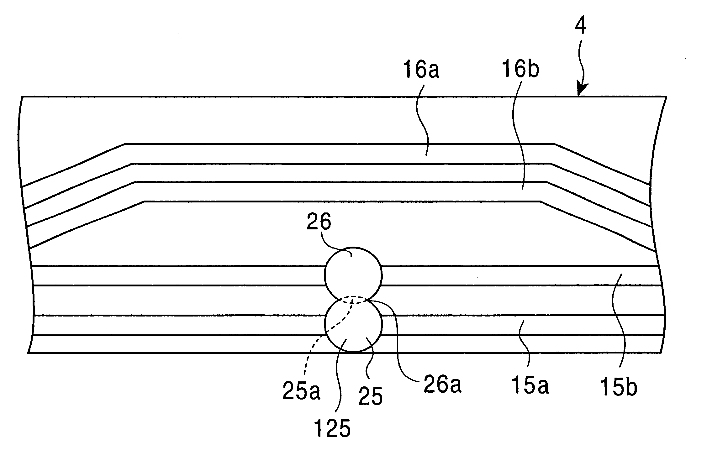
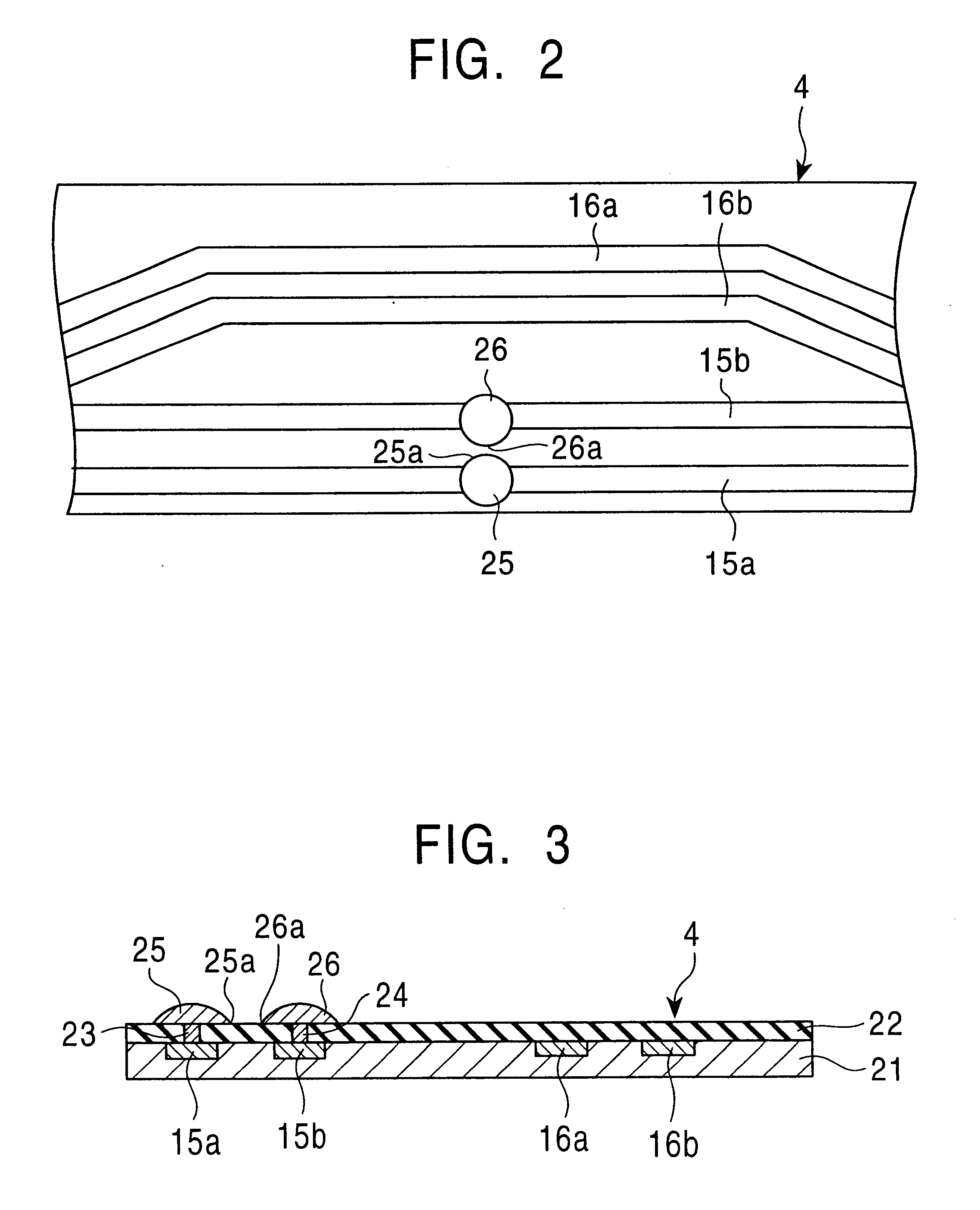
A land was formed on a circuit board, and a substantially semispherical solder bump having a diameter of 0.32 mm (320 .mu.m) and a maximum height of 28 .mu.m was formed on the land.

Further, on another circuit board, a substantially semispherical solder bump having a diameter of 0.26 mm (260 .mu.m) and a maximum height of 25 .mu.m was formed in a similar manner to the above. The solder used was made of an SnPb alloy and had the melting point of 183.degree. C.

These solder bumps were each crushed by applying a load of 5-15 kgf, and changes in the bump diameter were measured. Measured results are shown in FIGS. 14 and 15.

As seen from FIG. 14, the diameter of the solder bump having a diameter of 320 .mu.m was changed to 450-490 .mu.m after the crushing.

Also, as seen from FIG. 15, the diameter of the solder bump having a diameter of 260 .mu.m was changed to 370-430 .mu.m after the crushing.

It is thus understood that, when the solder bump is crushed, the bump diameter is increased and a p...


PUM

PropertyMeasurementUnit
diameteraaaaaaaaaa
diameteraaaaaaaaaa
melting pointaaaaaaaaaa

Abstract

The invention provides a magnetic head capable of positively preventing electrostatic breakdown of an MR magnetic head device, and a method of manufacturing the magnetic head. A circuit board comprises at least a pair of leads for constructing a circuit, lands connected respectively to the leads, and solder bumps formed respectively on the lands. The solder bumps are arranged in an adjacent relationship and, when the solder bumps are crushed, peripheral portions of the solder bumps are pressed or spread so as to overlap with each other. The magnetic head includes the circuit board.

Description

1. Field of the InventionThe present invention relates to a circuit board, and a magnetic head incorporating the circuit board. More particularly, the present invention relates to a circuit board capable of protecting an MR magnetic head device, which incorporates the circuit board, against electrostatic breakdown.2. Description of the Related ArtAn example of a conventional magnetic head 201 for use in a computer hard disk is shown in FIG. 17. The magnetic head 201 generally comprises a slider 203, a load beam 202, and a circuit board 204. The slider 203 is attached to a fore end 202a of the load beam 202 through a flexure, and a base plate 209 is attached to an opposite end 202b of the load beam 202. The circuit board 204 is attached to the base plate 209.The slider 203 includes an MR magnetic head device 208 for reproducing magnetically recorded data, and an inductive head device (not shown) for recording data to be magnetically recorded. From each of these head devices, two lead...

Claims


Application Information

Patent Timeline
Patent Type & Authority Patents(United States)
IPC IPC(8): G11B5/39G11B5/48G11B5/40H05K1/00G11B5/31H05K3/34H05K1/02
CPCG11B5/3903G11B5/40G11B5/4833G11B5/486H05K1/0293G11B5/3103H05K1/0259H05K3/3457H05K2201/0305H05K2203/0195H05K2203/0278H05K2203/173
Inventor MOTONISHI, MICHIHARUMOROE, MICHIAKI
Owner TDK CORPARATION
Why Eureka
Try Eureka