Method and structure for buried circuits and devices

a technology of buried circuits and devices, applied in the direction of semiconductor devices, semiconductor/solid-state device details, electrical apparatus, etc., can solve the problems of floating body effects, soi techniques introduce newer problems, and typically at higher manufacturing costs

Inactive Publication Date: 2004-07-06
GLOBALFOUNDRIES U S INC
View PDF33 Cites 282 Cited by
  • Summary
  • Abstract
  • Description
  • Claims
  • Application Information

AI Technical Summary

Problems solved by technology

Silicon-On-Insulator (SOI) technology has emerged as an electronic fabrication technique that improves characteristics such as latchup and speed, although typically at higher manufacturing cost.
The problem with this approach is that, although devices and interconnects are formed similar to conventional substrates, SOI techniques introduce newer problems such as floating body effects.
Additionally, conventional SOI structure takes up considerably more chip "real estate" than required in corresponding non-SOI structure, since floating body effects which not an issue with conventional substrates require additional connections to the channel regions.
More important, the conventional approach fails to recognize that the insulator layer could provide more functionality than merely separating predetermined groups of devices from the substrate.

Method used


Image

  • Method and structure for buried circuits and devices
  • Method and structure for buried circuits and devices
  • Method and structure for buried circuits and devices

Examples


Embodiment Construction

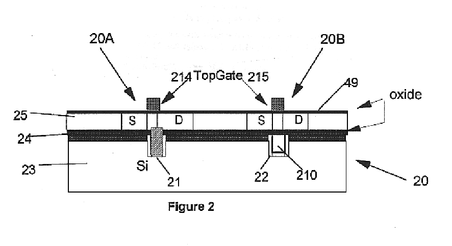
Going back to FIGS. 11A-11B illustrating the conventional SOI device, wherein oxide layer 111 separates device layer 110 from substrate 112. FET devices 113 are built into device layer 110. One conventional technique forms FET transistors with the following steps: a gate oxide is formed by a surface oxidation of layer 110, a gate electrode is formed by deposition and patterning of polysilicon, and source and drain regions are formed by implantation of a dopant. These source / drain regions, gate electrodes can then be surface wired 114 by common interconnection processes.

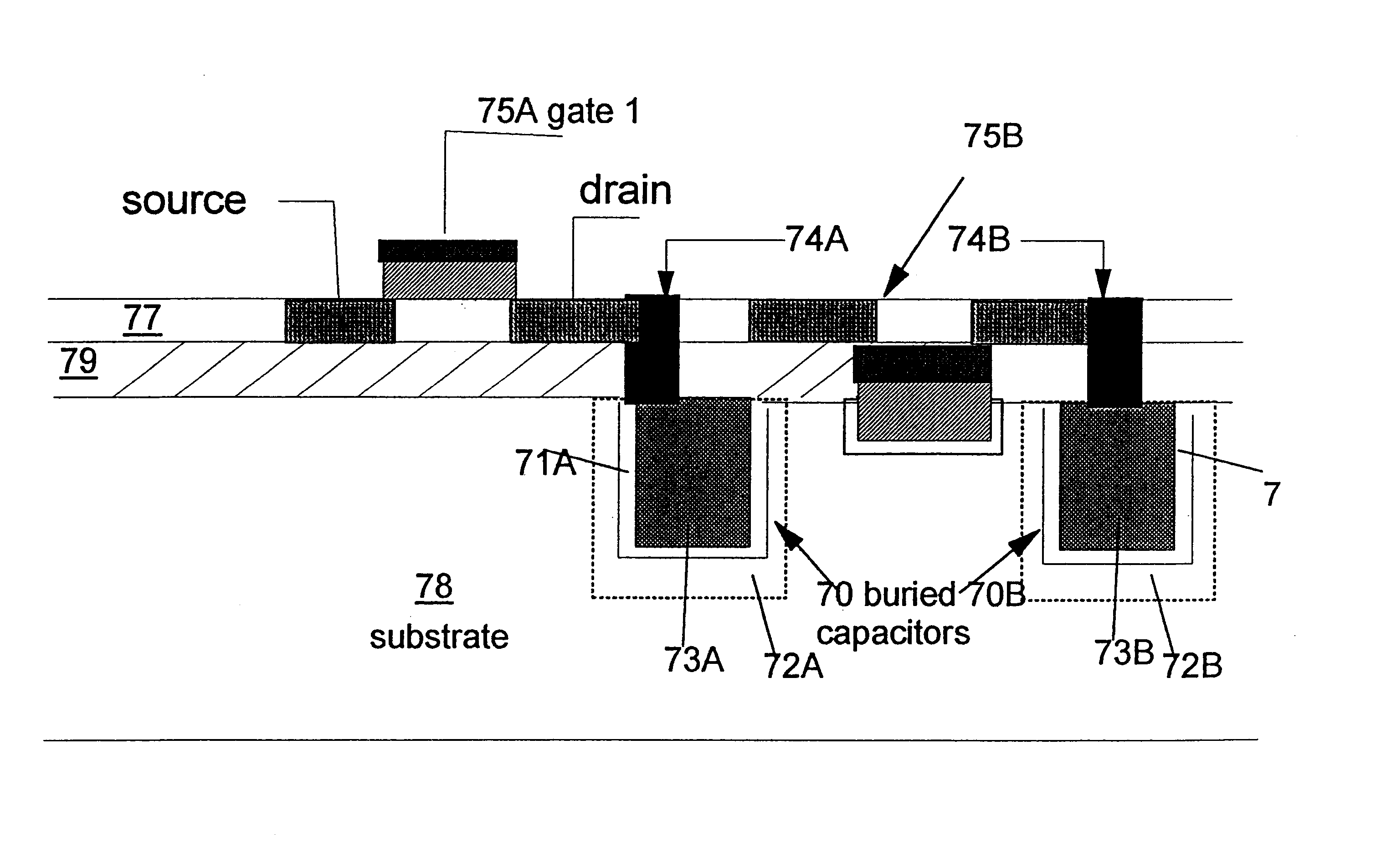
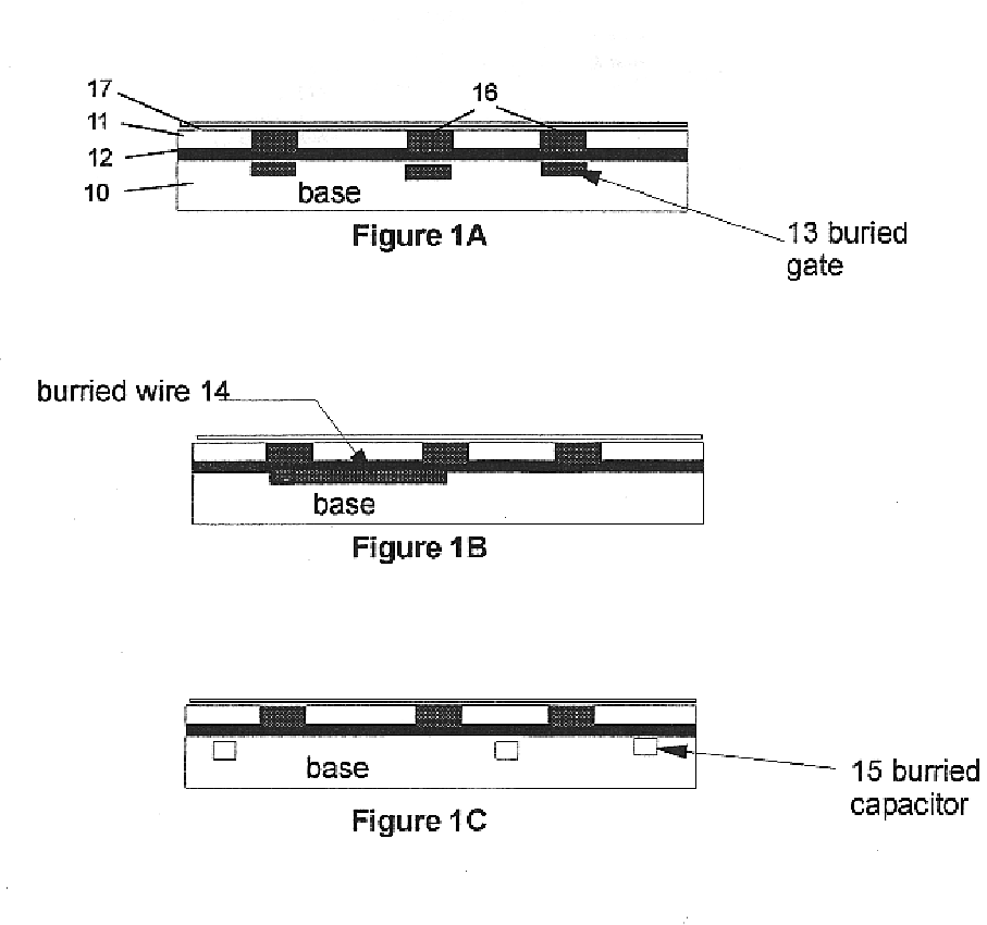
Turning now to the invention, FIGS. 1A-1C illustrate respectively a buried gate 13, a buried wire 14, and a buried capacitor 15 which are exemplary structures resulting from the present invention to use the BOX 12 as an integral part of devices and even entire circuits. Either the SIMOX technique or the bonded technique can be used. Substrate 10 receives device components which are then complemented with components 16...


PUM


Abstract

A method and structure for fabricating an electronic device using an SOI technique that results in formation of a buried oxide layer. The method includes fabricating at least one first component of the electronic device and fabricating at least one second component of the electronic device, wherein the first component and the second component are on opposite sides of the buried oxide layer, thereby causing the buried oxide layer to perform a function within the electronic device. Entire circuits can be designed around this technique.

Description

1. Field of the InventionThe present invention involves fabrication of semiconductor devices using Silicon-on-Insulator (SOI) technology. More specifically the invention is directed to the use of the SOI Buried Oxide (BOX) layer as an integral component of electronic devices and circuits.2. Description of the Related ArtSilicon-On-Insulator (SOI) technology has emerged as an electronic fabrication technique that improves characteristics such as latchup and speed, although typically at higher manufacturing cost. The term SOI typically describes structures where devices are fabricated in single-crystal Si layers formed over an insulating film or substrate.FIGS. 11A and 11B show a typical conventional SOI structure, where a thin silicon device layer 110 formed on an insulator 111 is supported over substrate 112. For current technology the substrate is most commonly silicon and the insulator is most commonly silicon dioxide. Devices 113 are formed in device layer 110 and interconnected ...

Claims


Application Information

Patent Timeline
Patent Type & Authority Patents(United States)
IPC IPC(8): H01L21/762H01L21/70H01L27/108H01L27/12H01L21/8242H01L21/84H01L21/02H01L21/3205H01L21/336H01L21/76H01L21/8234H01L21/8238H01L23/52H01L27/06H01L27/08H01L27/088H01L27/092H01L27/118H01L29/786
CPCH01L21/743H01L21/76251H01L21/84H01L27/10832H01L27/10873H01L27/11803H01L27/1203H01L29/66772H01L29/78606H01L29/78612H01L29/78648H01L2924/0002H01L2924/00H10B12/373H10B12/05H10B99/00
Inventor CAMPBELL, JOHN E.DEVINE, WILLIAM T.SRIKRISHNAN, KRIS V.
Owner GLOBALFOUNDRIES U S INC
Why Eureka
Try Eureka