Pattern correction method, apparatus, and program

a technology of program and correction method, applied in the field of pattern correction method, can solve the problems of poor correction accuracy, large time requirement for graphics processing and distance calculation for opc processing, and the prevention of yield reduction

Inactive Publication Date: 2004-09-14
KK TOSHIBA
View PDF11 Cites 224 Cited by
  • Summary
  • Abstract
  • Description
  • Claims
  • Application Information

AI Technical Summary

Problems solved by technology

Accompanying the miniaturization and increased integration of semiconductor integrated circuits, prevention of decreases in yield due to the optical proximate effect during the photolithography process has become an important issue.
In the case of a large-scale integrated circuit, since the number of metal interconnects and VIA graphics is huge, a great deal of time is required to perform graphics processing and distance calculation for the OPC processing.
As a result, correction accuracy is poor, and ultimately satisfactory accuracy cannot be achieved in the post-exposure pattern created.

Method used


Image

  • Pattern correction method, apparatus, and program
  • Pattern correction method, apparatus, and program
  • Pattern correction method, apparatus, and program

Examples


first embodiment

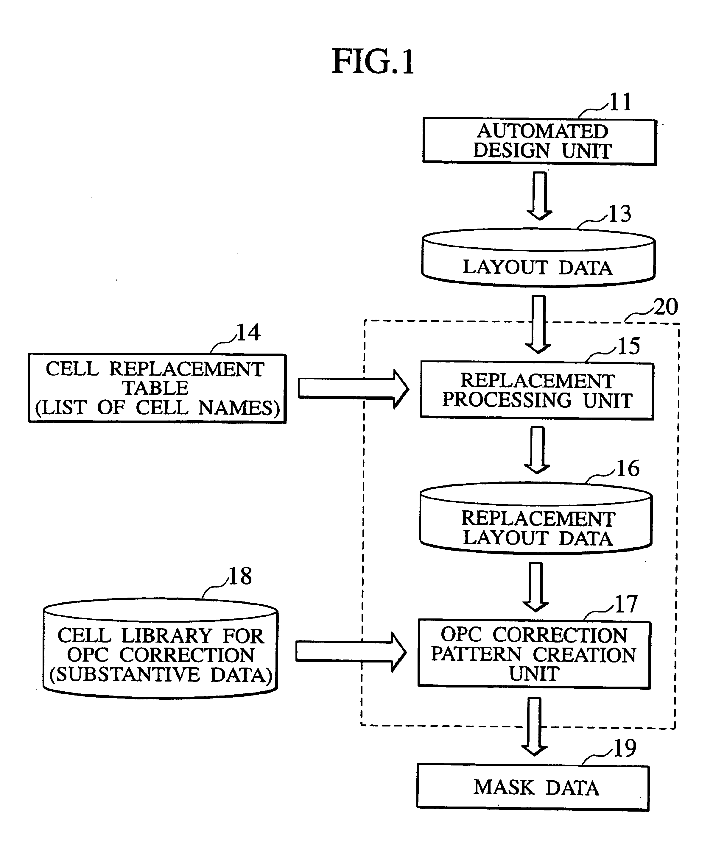
FIG. 1 illustrates an outline of optical proximity correction (OPC) according to the first embodiment of the present invention. OPC is initiated by entering layout data 13 created by an automated design unit 11, such as CAD, into an OPC correction processing unit 20. The OPC correction processing unit 20 applies pattern correction to layout data 13, such as an interconnect pattern designed with CAD, in anticipation of the optical proximate effect caused by the exposure a micro pattern.

During this pattern correction, the input design layout data 13 is converted to replacement layout data 16 by a replacement processing unit 15 while referencing a cell replacement table 14. The replacement layout data is transmitted to an OPC correction pattern creation unit 17. Referencing a cell library 18 for OPC correction, the OPC correction pattern creation unit 17 imports a substantive post-correction pattern and outputs mask data 19.

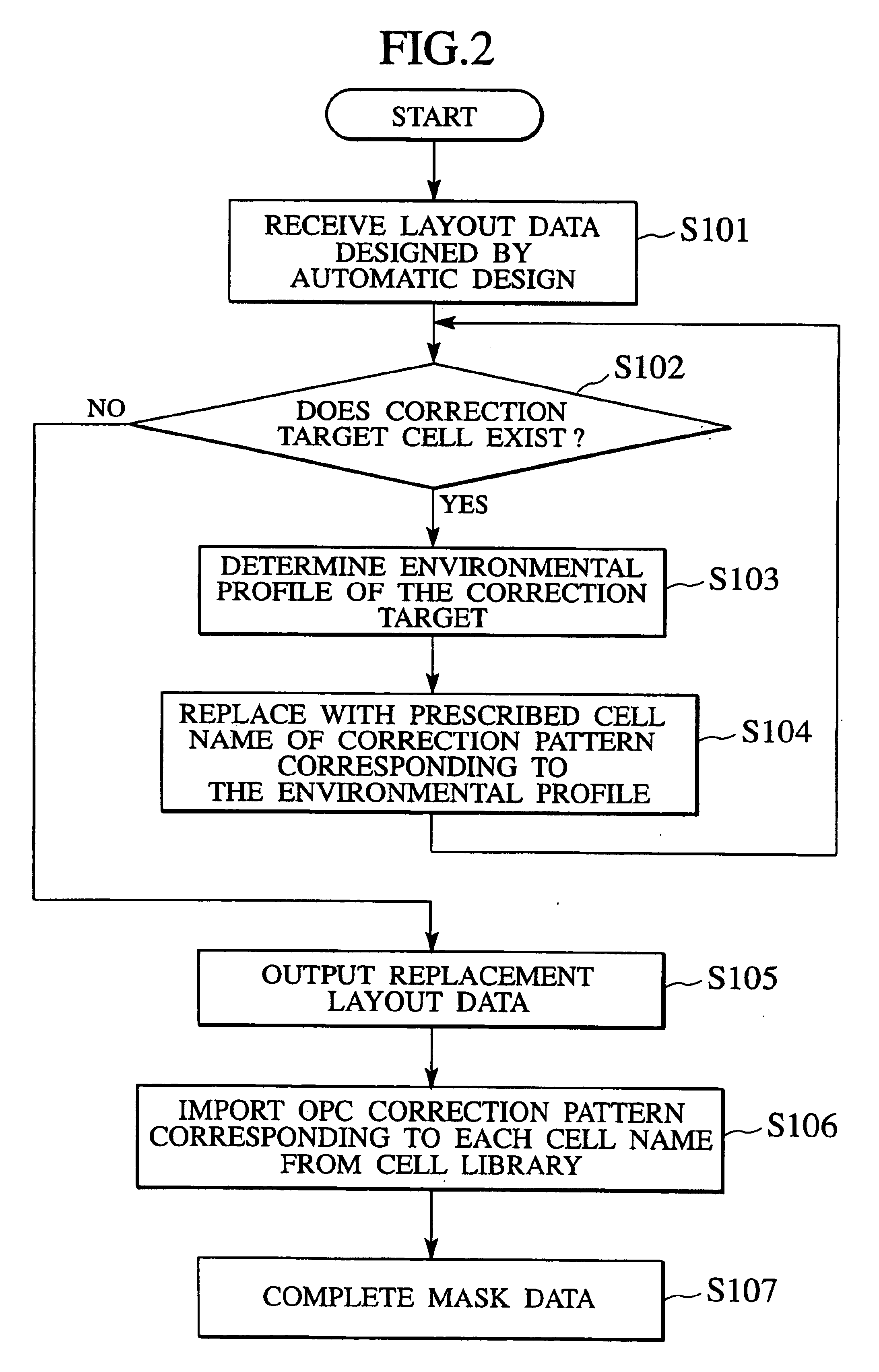
FIG. 2 is a more specific processing flow chart for the OPC co...

second embodiment

In the first embodiment, the correction of multi-level interconnect patterns in the rectangular coordinate system was described. In the second embodiment, pattern correction for diagonal interconnect is described while referencing FIGS. 11 to 13.

The case where the lower-level metal interconnect extends toward the prescribed direction (e.g., horizontal direction) on the rectangular coordinate system and the upper-level metal interconnect at the upper level extends toward diagonal direction at the prescribed angle with the lower-level horizontal interconnect is considered.

FIG. 11 illustrates segments for determining the environmental profile for the upper-level metal interconnect 121, which constructs the VIA cells, and FIG. 12 illustrates segments for determining the environmental profile for the lower-level metal interconnect 123. In the second embodiment, the cross-sectional shape of VIA contacts 122, which connect the upper-level diagonal interconnect 121 and lower-level horizonta...

third embodiment

FIG. 14 is a diagram of an OPC pattern correction apparatus according to a third embodiment of the present invention. The pattern correction apparatus 150 comprises a CPU (correction processing unit) 151; memory 152; and an input / output unit 153. A design pattern designed with an automated layout unit, such as CAD, is input to the pattern correction apparatus 150 via the input / output unit 153.

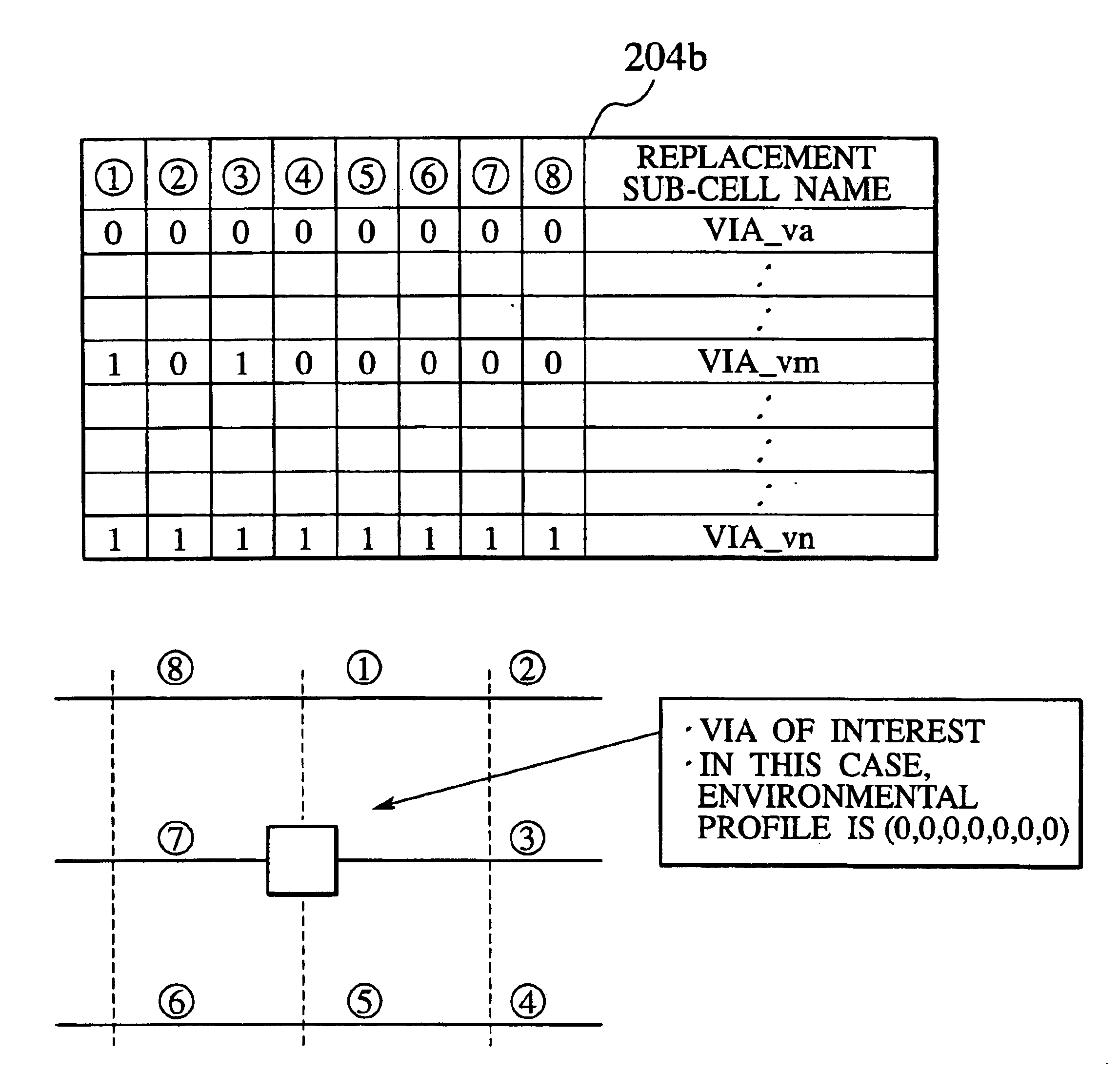
The memory 152 stores a cell replacement table 157 and a cell library 158 for OPC correction. The cell replacement table 157 indexes all possible environmental profiles with the names (referred to as cell names) representing the most appropriate correction shape corresponding to each environmental profile in relation to the pattern (target cell) to be corrected and stores them. The cell library 158 for OPC correction stores the actual correction pattern data indicated by the cell names in the cell replacement table 157.

The CPU 151 comprises an environmental profile determination unit 154; a rep...


PUM

PropertyMeasurementUnit
optical proximity correctionaaaaaaaaaa
widthaaaaaaaaaa
VIA resistanceaaaaaaaaaa

Abstract

In a pattern correction method, design layout data of a pattern designed by an automated layout unit is entered. An environmental profile is determined based on whether or not another graphics pattern exists at the surroundings of each correction target cell included in the entered design layout data. A target cell name is replaced with a prescribed cell name of correction pattern corresponding to the determined environmental profile by referencing a cell replacement table. An OPC correction pattern corresponding to the replaced cell name is imported from a cell library.

Description

1. Field of the InventionThe present invention relates to a pattern correction method, which corrects layout data for a circuit pattern of a semiconductor integrated circuit, and a pattern correction apparatus. In particular it relates to an optical proximity correction (OPC) pattern correction method, which corrects for the optical proximate effect, and a pattern correction apparatus.2. Description of the Related ArtAccompanying the miniaturization and increased integration of semiconductor integrated circuits, prevention of decreases in yield due to the optical proximate effect during the photolithography process has become an important issue. More specifically, in the case of forming a circuit pattern using the photolithography process, due to the optical proximate effect, the edge of the actually exposed and finished interconnect pattern is shortened in comparison with layout patterns such as those designed using computer-aided design (CAD) system. This phenomenon is called "sho...

Claims


Application Information

Patent Timeline
Patent Type & Authority Patents(United States)
IPC IPC(8): G03F1/14G03F1/36G03F1/68
CPCG03F1/144G03F1/36
Inventor TAKASHIMA, MAKOTOIKEUCHI, ATSUHIKOHASHIMOTO, KOJIIGARASHI, MUTSUNORIYAMADA, MASAAKI
Owner KK TOSHIBA
Why Eureka
Try Eureka