Dual gate low noise amplifier

a low-noise amplifier and dual-gate technology, applied in the direction of low-noise amplifiers, amplifiers with field-effect devices, gain control, etc., can solve the problems of increasing noise, introducing additional unwanted noise into the amplifier output, and often having to reach compromise between the end goals, so as to improve performance and achieve low noise. the effect of figure and high gain

Inactive Publication Date: 2004-10-05
NORTHROP GRUMMAN SYST CORP
View PDF3 Cites 15 Cited by
  • Summary
  • Abstract
  • Description
  • Claims
  • Application Information

AI Technical Summary

Benefits of technology

Such an arrangement enables improved performance, including low noise figure and a high gain, compared to conventional amplifiers designed to achieve similar gain. Additionally, an amplifier can be implemented according to an aspect of the present invention as a single stage amplifier on a single chip, occupying less real estate relative to conventional amplifier designs.
Another aspect of the present invention provides a method for implementing a low noise amplifier. The method includes providing a dual gate transistor device connected between an input and an output of the amplifier. Resistive feedback is provided between the output and a first gate of the transistor device and electrically connected with the input of the amplifier to provide the amplifier with a desired gain. The feedback also includes a DC blocking component in series with a resistive part of the resistive feedback. To operate the amplifier, the first gate of the transistor device is biased with a first DC voltage, such as through a node associated with the resistive feedback. A second gate of the transistor device is biased with a second DC voltage that is greater than the first voltage. As a result, a low noise figure (e.g., less than about 1 dB) can be achieved for the amplifier over a desired frequency range.

Problems solved by technology

Broadband amplifiers of this type tend to employ feedback paths that introduce additional unwanted noise into the amplifier output.
While the Darlington pair resistive feedback amplifier is traditionally used for medium to high gain applications, the current gain and base resistance of the active device tend to limit the noise figure.
These and other conventional amplifier approaches usually fail to optimize source impedance matching for microwave devices, which also can result in added noise.
As a result, a compromise often must be reached between the end goals, which can be conflicting at times.

Method used


Image

  • Dual gate low noise amplifier
  • Dual gate low noise amplifier
  • Dual gate low noise amplifier

Examples


Embodiment Construction

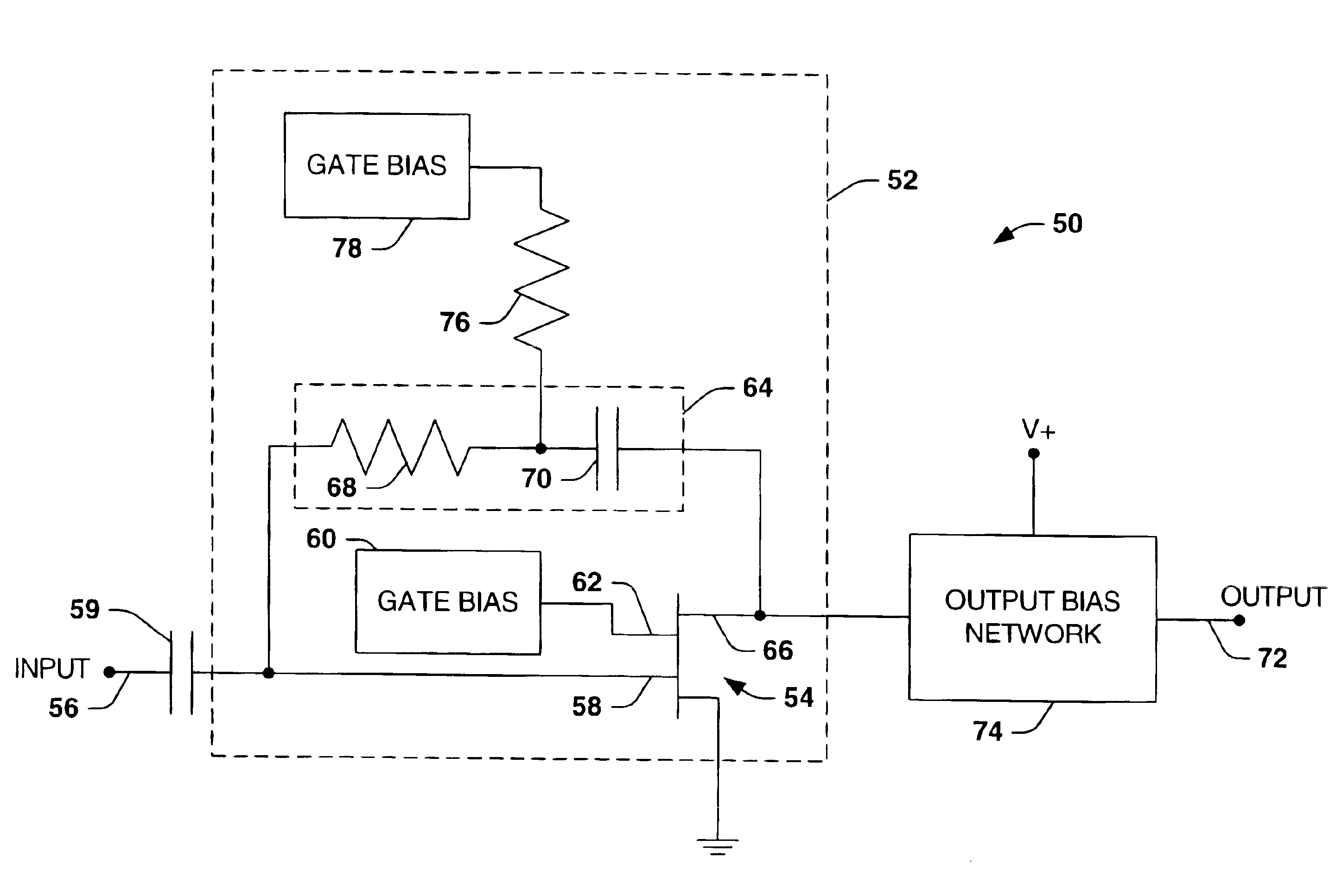
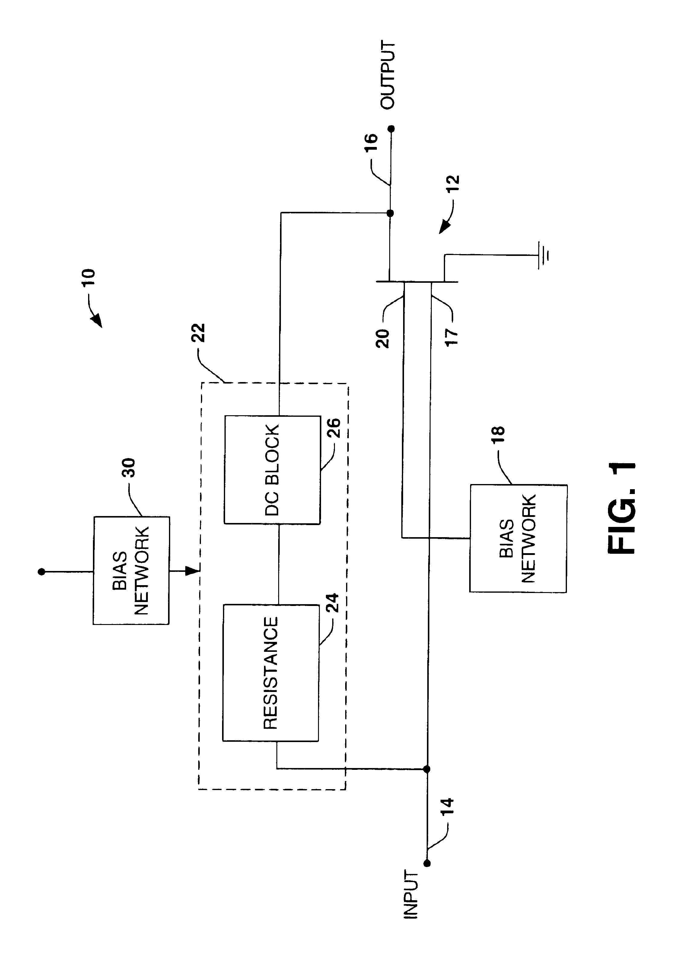
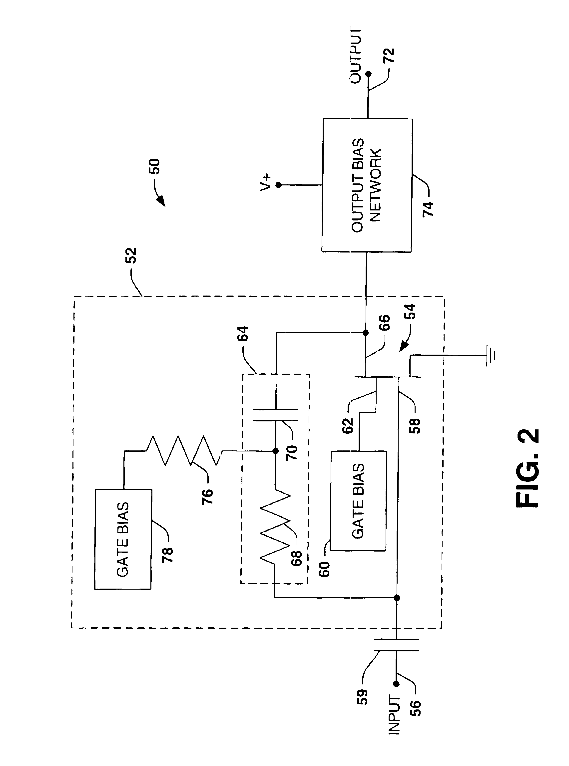
The present invention relates to a low noise amplifier topology that can be implemented with a dual gate high electron mobility transistor (HEMT) device. The amplifier employs resistive feedback with a DC block associated with the amplifier output to provide desired high voltage gain and a low noise figure for desired frequencies, such as generally in the range of VHF and microwave frequencies.

FIG. 1 illustrates a schematic example of a low noise amplifier 10 in accordance with an aspect of the present invention. The amplifier 10 includes a dual gate transistor device 12 that is coupled to an input 14 for receiving a RF input signal. The transistor device 12 is operative to amplify the RF input signal and provide an amplified output signal at an associated output 16.

The transistor device 12 can be a dual gate field effect transistor (FET) fabricated to provide high electron mobility (e.g., a high electron mobility transistor (HEMT) device). A dual gate HEMT device affords increased ...


PUM


Abstract

A low noise amplifier topology includes a dual gate transistor device, such as a HEMT device and employs resistive feedback with a DC block associated with the amplifier output to a desired high voltage gain and a low noise figure over a desired range of frequencies.

Description

The present invention relates generally to signal amplification, and more particularly to a dual gate amplifier having low noise characteristics.A low noise amplifier (LNA) is utilized in various aspects of wireless communications, including wireless LANs, cellular communications, and satellite communications. A LNA is often utilized in an input stage of a signal receiving apparatus or receiver. For example, the LNA amplifies a received RF (Radio Frequency) input signal so that an amplified RF signal has a desired gain and noise figure.Two main concerns associated with the design of amplifiers utilized for low noise RF amplification include: (1) the minimization of noise added to the signal by the amplifier; and (2) achieving maximum power transfer between a source producing the electrical signal and the amplifier. A figure of merit for noise added by the amplifier is the ratio of the signal-to-noise ratio at the input to the signal-to-noise ratio at the output of the amplifier. Thi...

Claims


Application Information

Patent Timeline
Patent Type & Authority Patents(United States)
IPC IPC(8): H03F1/08H03F1/22H03F1/30H03F1/34H03F3/193H03F1/26
CPCH03F1/226H03F1/306H03F1/342H03F2200/372H03F2200/294
Inventor ALLEN, BARRY R.CHUNG, YUN H.BRUNONE, DAVID J.
Owner NORTHROP GRUMMAN SYST CORP
Why Eureka
Try Eureka