Unlock instant, AI-driven research and patent intelligence for your innovation.

Implementation method of an all-optical half adder by using SOA-based devices and an apparatus thereof

an all-optical, half-adder technology, applied in the direction of computation using denominational number representation, pulse technique, instruments, etc., can solve the problems of increasing the demand for high-speed and large-scale communication systems, limiting the operation speed and information handling capacity of most current-use communication systems based on silicon (si) material (i.e. based on electric signals), and achieving small system size, easy to be combined with other optical devices

Inactive Publication Date: 2004-10-05
KOREA INST OF SCI & TECH
View PDF8 Cites 12 Cited by
  • Summary
  • Abstract
  • Description
  • Claims
  • Application Information

AI Technical Summary

Benefits of technology

The solution provides a stable, compact, and highly integrated all-optical half adder capable of operating at high speeds, overcoming integration challenges and achieving efficient logic operations, thus enhancing the performance of communication systems.

Problems solved by technology

Demand of high-speed and large-scale of a communication system is recently being increased, however, most of currently used communication systems based on silicon (Si) material (i.e. based on electric signal) have limitations in their operation speed and information handling capacity.
And thus, the future performance of this type of communication system is questionable.
As the complexity of the communication system increases, the multiple operations of logic gates are required.
However, the key components of these systems are optical fibers that are complicated and hard to be integrated with other devices, and thus, they have difficulties in being applied to an optical computation system requiring a highly integrated circuit.
And, an implementation method using a four-wave mixing has a problem that it is hard to control the polarization state of a signal.

Method used


Image

  • Implementation method of an all-optical half adder by using SOA-based devices and an apparatus thereof
  • Implementation method of an all-optical half adder by using SOA-based devices and an apparatus thereof
  • Implementation method of an all-optical half adder by using SOA-based devices and an apparatus thereof

Examples


Embodiment Construction

As described above, the present invention is characterized in that SUM signal is outputted by adding the output signals of inverter characteristic produced by gain-saturation and wavelength conversion of semiconductor optical amplifier (SOA) by injecting both pump signal and probe signal together into each semiconductor optical amplifier; and CARRY signal, of which the power of output signal is being increased by simultaneously injecting a high-power probe signal into an XPM wavelength converter with varying a pump signal and the power of output signal is being decreased by simultaneously injecting a low-power probe signal into an XPM wavelength converter with varying a pump signal, is outputted.

Hereinafter, referring to appended drawings, the embodiments of the present invention are described in detail.

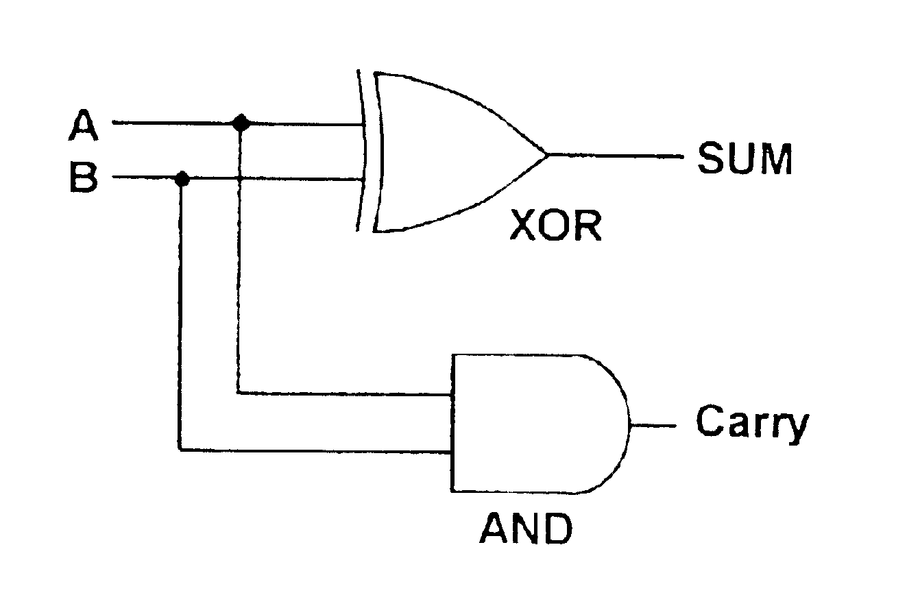
FIG. 1 is a view illustrating the basic concept of a half adder.

A half adder described in FIG. 1 is a system producing the signals of SUM represented by Table 1 and CARRY represented...


PUM

PropertyMeasurementUnit
poweraaaaaaaaaa
opticalaaaaaaaaaa
optical delayaaaaaaaaaa

Abstract

The present invention relates to an implementation method of all-optical half adder by using semiconductor optical amplifier(SOA)-based devices and the apparatus thereof. In more detail, it relates to an implementation method of all-optical half adder comprising an all-optical XOR gate and an all-optical AND gate, implemented by using SOA-based devices, and an apparatus thereof.

Description

1. Field of the InventionThe present invention relates to an implementation method of all-optical half adder by using semiconductor optical amplifier (SOA)-based devices and the apparatus thereof. In more detail, it relates to an implementation method of all-optical half adder comprising an all-optical XOR gate and an all-optical AND gate, implemented by using SOA-based devices, and an apparatus thereof.2. Description of the Related ArtDemand of high-speed and large-scale of a communication system is recently being increased, however, most of currently used communication systems based on silicon (Si) material (i.e. based on electric signal) have limitations in their operation speed and information handling capacity. And thus, the future performance of this type of communication system is questionable.On the other hand, a communication system using optical devices based on indium phosphide (InP) can solve the problems of operation speed and information handling capacity described abo...

Claims


Application Information

Patent Timeline
Patent Type & Authority Patents(United States)
IPC IPC(8): G02F3/00H01S5/50H01S5/00H01S3/06H01S3/067G06F7/48G06E1/04
CPCG02F3/00H01S5/50H01S5/509H01S3/06754G06F7/48
Inventor KIM, JAE HUNBYUN, YOUNG TAEJHON, YOUNG MINLEE, SEOKWOO, DEOK HAKIM, SUN HO
Owner KOREA INST OF SCI & TECH