

Delay compensation circuit
a delay compensation and circuit technology, applied in the direction of generating/distributing signals, instruments, pulse techniques, etc., can solve the problems of clock signals arriving earlier than expected, data signals violating the setup time, other types of synchronous logic elements,
- Summary
- Abstract
- Description
- Claims
- Application Information
AI Technical Summary
Benefits of technology
Problems solved by technology
Method used
Image

Examples
Embodiment Construction
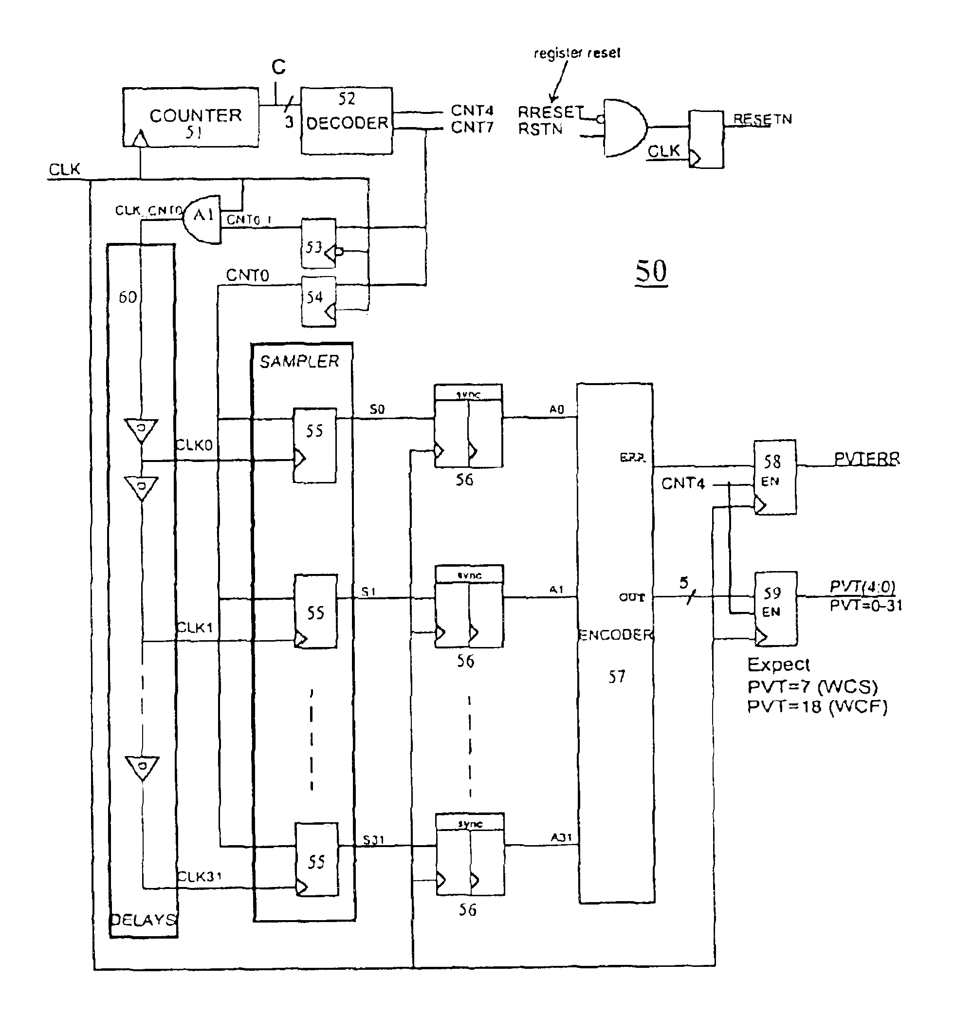
As described above, the present invention is directed to a delay compensation circuit, which measures the effects of PVT variations on a chip by measuring variations in the delay time of a delay component in the chip. The delay compensation circuit of the present invention can be utilized to program the delay time of a variable delay component and for providing information to be used in chip design to compensate for PVT conditions. Many of the figures referred to in connection with this detailed description contain similar components. The same reference labels will be used throughout the figures to denote similar components.
FIG. 5 illustrates a delay compensation circuit 50 according to an exemplary embodiment of the present invention. An external clock signal CLK is connected to counter 51, an input of logical AND gate A1, sampling modules 53 and 54, synchronizers 56, and latches 58 and 59. The output C of counter 51 is connected to decoder 52. Output CNT4 of the decoder 52 is conn...
PUM
 Abstract
Description
Claims
Application Information