High speed multi-stage switching network formed from stacked switching layers

a multi-stage switching and switching layer technology, applied in the field of data switches, can solve the problems of difficult to achieve wire-speed routing at higher data rates, difficult to build bus arbitration schemes fast enough to provide non-blocking performance at multigigabit speeds, and limited data rate and port count capacity

Inactive Publication Date: 2004-12-07
NYTELL SOFTWARE LLC
View PDF15 Cites 93 Cited by
  • Summary
  • Abstract
  • Description
  • Claims
  • Application Information

AI Technical Summary

Problems solved by technology

While this simple bus-based, software controlled architecture is useful for a router with 10 megabits per second (Mbps) ports, and perhaps for a router with relatively few 100 Mbps ports, its capacity is limited in terms of data rate and port count.
It is difficult to achieve wire-speed routing at higher data rates with this architecture because of bottlenecks associated with the shared bus, the memory's data transfer bandwidth, and the processor's clock speed.
According to one author, "it is almost impossible to build a bus arbitration scheme fast enough to provide nonblocking performance at multigigabit speeds."
Crossbar switches are conceptually desirable, but they have generally been regarded as physically impractical for large switches.
Crossbars usually have very low blocking probabilities, but they have a key defect: they require a lot of circuitry (proportional to n.sup.2 or worse) in each output port.
In other words, prior art approaches to crossbar switches do not scale well such that they are generally regarded as useful only for small switches:
Unfortunately, an N.times.N crossbar uses N.sup.2 elements and therefore is expensive for large N, such as N=100,000 *** However, crossbars are an excellent solution for building smaller (say, 8.times.8 or 64.times.64 switches).
Moreover, switch fabrics with even more columns are possible, but the return on investment for each additional column is marginal.
The groupings of signals through fewer stages providing less than the nonblocking number of switching elements introduces some small probability of internal blocking, but it is relatively small.
The inventors believe that designers have come to regard crossbar switches as impractical for creating large switches because the implementing electronics would occupy a large area and have long interconnects.
The problem is that the long interconnects exhibit parasitic losses that tend to make the switch relatively slow and inefficient at the same time that the switch must consume more power to overcome interconnect related losses.
It has not been practical until now, however, to use superconducting elements to make large switches with a large number of ports.
It is very impractical, however, to cool such a large area to superconducting temperatures of 120K (-243.67 degrees Fahrenheit) required for so-called "high-temperature superconductors" or, for that matter, to even lower temperatures such as 4K (-452.47 degrees Fahrenheit) required for other superconducting technologies.
A large multi-stage switch constructed from a planar arrangement of switching elements on a PCBA, therefore, is impractical because the assembly is physically large, operationally slow and, were it desired to do so, difficult to cool to superconducting temperatures.
A large switch of conventional construction consumes excessive space because the physical size of the PCBA grows quadratically with the number of inputs and outputs.
A large switch formed from building blocks of conventional construction would operate at less than optimal clock speeds because of increased signal latency due to parasitic loads present over long lines.
A large switch of conventional construction would be difficult to implement with superconducting electronics with individual building blocks distributed over a relatively large PCBA. because the relatively large size of the PCBA is not amenable to being cooled to superconducting temperatures, , and because the PCBA layers and dissimilar materials are in contact with one another.
In summary, as a conventional crossbar switch grows with electronics of conventional construction, it becomes slower and burns more power due the parasitic losses associated with the growing length of interconnects.
At the same time, the growing switch area becomes increasingly difficult to cool to the superconducting temperatures needed to implement the switch with high speed, low power electronics of superconducting construction.

Method used


Image

  • High speed multi-stage switching network formed from stacked switching layers
  • High speed multi-stage switching network formed from stacked switching layers
  • High speed multi-stage switching network formed from stacked switching layers

Examples


Embodiment Construction

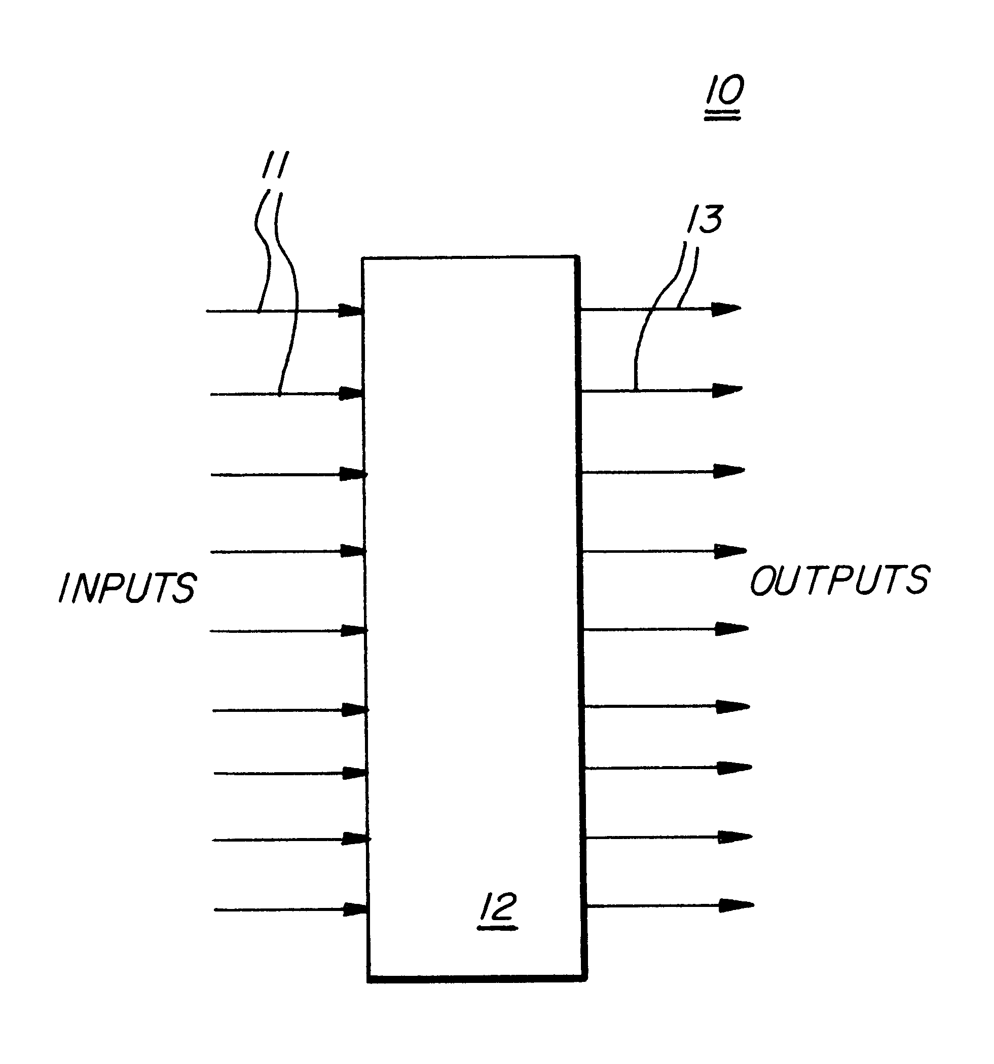
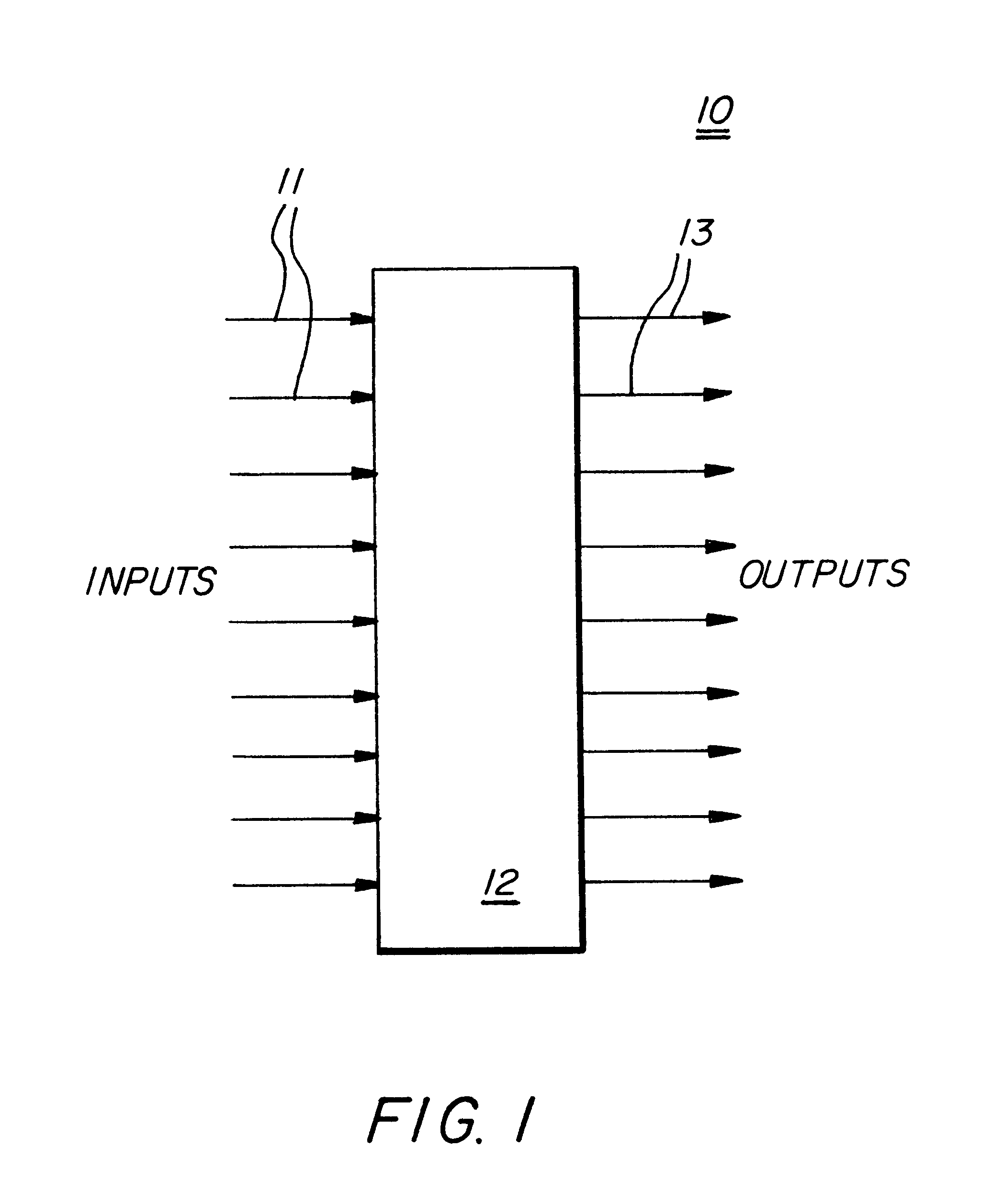
FIG. 7 shows a simplified block diagram of a high speed, compact, multi-stage switching network 100 according to a first preferred embodiment of this invention. The switching network 100 is, as shown, adapted for simultaneously routing a plurality of data packets from a first plurality of electronic data input ports 110 to selected ones of a second plurality of electronic data output ports 190.

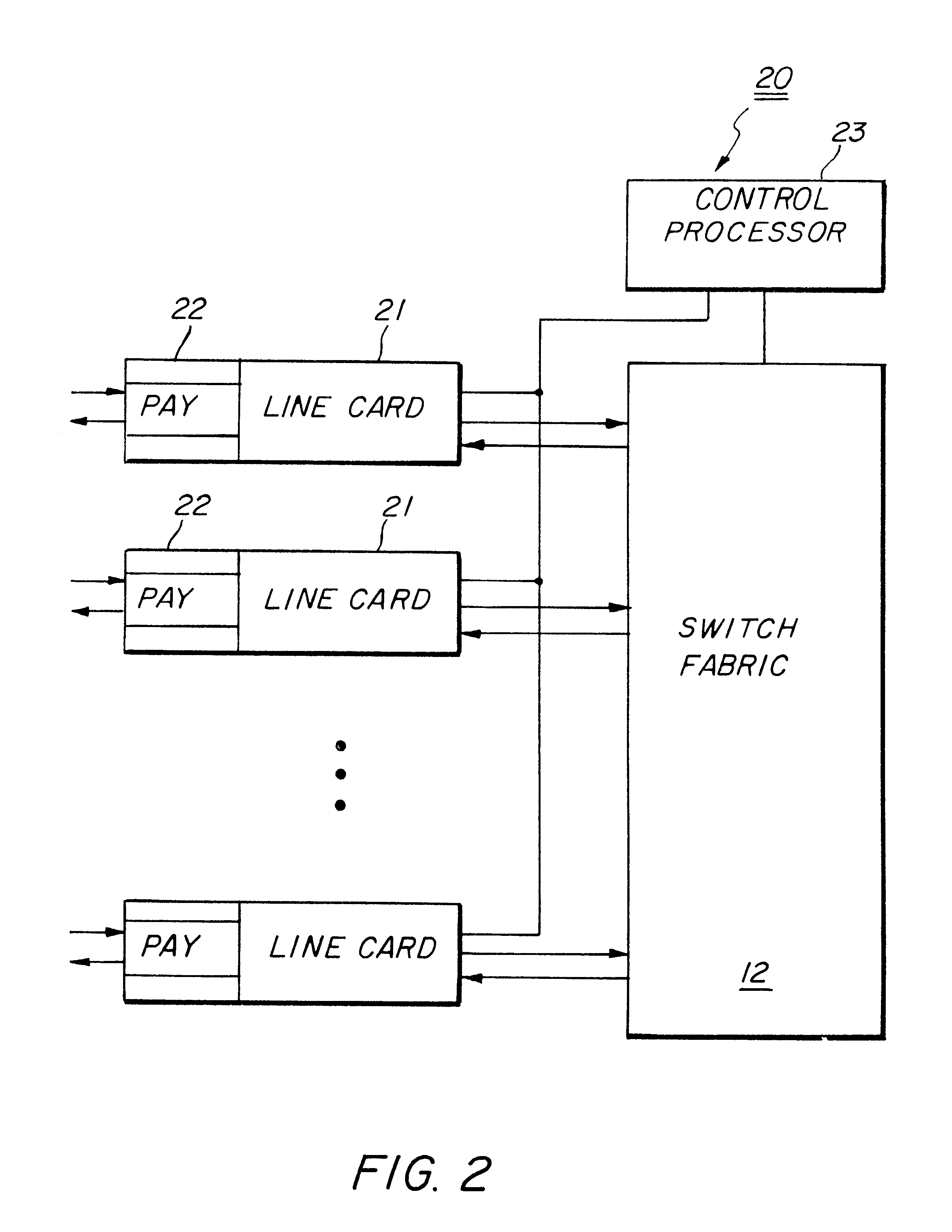
The compact switching network 100 of this first preferred embodiment is formed from first and second stacks 140, 160 of IC switching layers 113 that are stacked in physical contact with one another, each IC switching layer 113 containing at least one switching element circuit (see e.g. 142, 162 of FIG. 10). The compact switching network 100 further comprises means 150 for interconnecting the interface conductors of the first stack 140 of IC layers to the interface conductors of the second stack 160 of IC layers to form the overall, compact multi-stage switching network 100.

The multi-stage swit...


PUM


Abstract

A compact multi-stage switching network (100), and a router (510) incorporating such multi-stage switching network, adapted for simultaneously routing a plurality of data packets from a first plurality of input ports (110) to selected ones of a second plurality of output ports (190) comprising: a first stack (140) of IC switching layers (113) that are stacked in physical contact with one another, each IC switching layer containing at least one switching element circuit (142); a second stack (160) of IC switching layers (113) that are stacked in physical contact with one another, each IC switching layer (113) containing at least one switching element circuit (162); and interconnecting circuitry (150) that connects the first stack (140) of IC layers to the second stack (160) of IC layers to form the compact multi-stage switching network. The stacks (140, 160) are preferably mated to one another in a transverse fashion in order to achieve a natural full-mesh connection. Also contemplated are the use of superconducting IC switching circuits (142) and a suitable superconducting cooling housing (730), as permitted by the compact nature of the multi-stage switching network (100), in order to operate at high speed and low power.

Description

1. Field of the InventionThis invention relates generally to data switches and, more specifically, to a high speed multi-stage switching network formed from stacked switching layers for use in routers and the like.2. Description of the Related ArtThis invention relates to switches. A switch, in the most general sense relevant here, is a communications device that controls the routing of a signal path. Switches are generally categorized as packet switches or as circuit switches. Packet switches, also sometimes called datagram switches, switch packets containing both data and meta-data (control information). Some well-known packet switching devices are IP routers and asynchronous transfer mode (ATM) switches. As stated in RFC 1812, "An IP router can be distinguished from other sorts of packet switching devices in that a router examines the IP protocol header as part of the switching process. It generally removes the Link Layer header a message was received with, modifies the IP header...

Claims


Application Information

Patent Timeline
Patent Type & Authority Patents(United States)
IPC IPC(8): H04L12/56G06T7/20G06T9/00
CPCG06T7/20G06T9/004H04L45/583H04L49/25H04L49/101H04L49/15Y10S257/93H04L49/3018H04L49/3027H04L49/351H04L49/357H04L49/1507
Inventor CARSON, JOHN C.OZGUZ, VOLKAN H.
Owner NYTELL SOFTWARE LLC
Why Eureka
Try Eureka