Method and apparatus for depositing and controlling the texture of a thin film

a thin film and texture technology, applied in the direction of manufacturing tools, semiconductor/solid-state device details, lapping machines, etc., can solve the problems of difficult to accelerate the growth of room temperature grain in the conductive layer b>8, and achieve the effects of reducing the annealing time, and reducing the annealing cos

Inactive Publication Date: 2005-01-04
NOVELLUS SYSTEMS
View PDF32 Cites 33 Cited by
  • Summary
  • Abstract
  • Description
  • Claims
  • Application Information

AI Technical Summary

Benefits of technology

[0024]In addition, energy stored in the cold worked regions or portions of the deposited layer is used to accelerate the grain recovery and growth. Thus, large grain size can be obtained in the deposited material at a lower annealing temperature and a shorter annealing time.

Problems solved by technology

Thus, it is very difficult to form grains in the conductive layer 8 that are different in their texture from the grains of the seed layer 6.
In addition, it is also difficult to accelerate room temperature grain growth of the conductive layer 8 without changing the texture of the seed layer 6, bath chemistry and / or temperature.

Method used


Image

  • Method and apparatus for depositing and controlling the texture of a thin film
  • Method and apparatus for depositing and controlling the texture of a thin film
  • Method and apparatus for depositing and controlling the texture of a thin film

Examples


Embodiment Construction

d polishing a conductive layer in accordance with the preferred embodiment of the present invention;

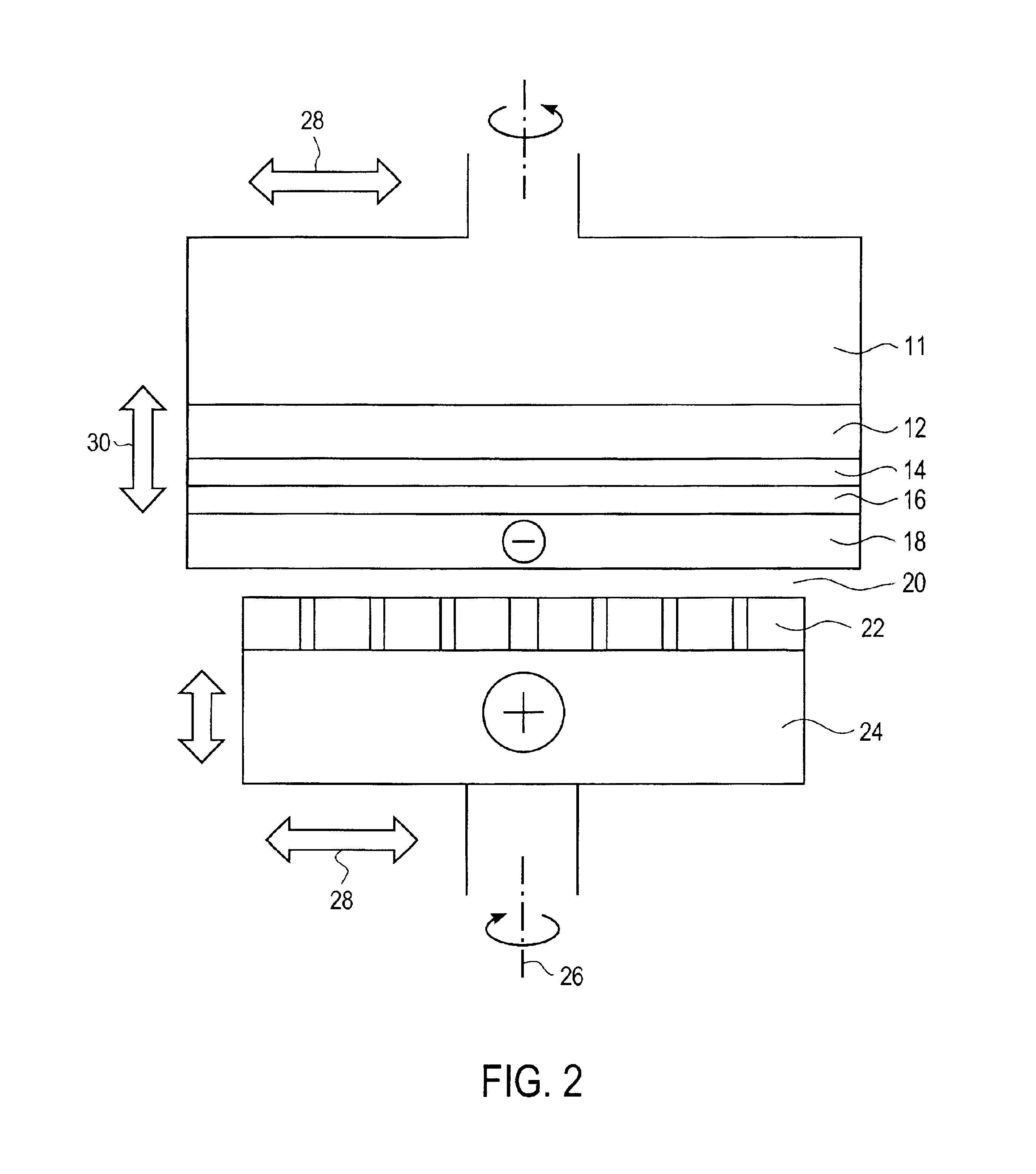
[0031]FIG. 5 illustrates a side view of an apparatus in accordance with the first preferred embodiment of the present invention;

[0032]FIG. 6 illustrates a side view of an apparatus in accordance with the second preferred embodiment of the present invention;

[0033]FIG. 7 illustrates a side view of an apparatus in accordance with the third preferred embodiment of the present invention;

[0034]FIG. 8 illustrates a side view of an apparatus in accordance with the fourth preferred embodiment of the present invention;

[0035]FIG. 9 illustrates a side view of an apparatus in accordance with the fifth preferred embodiment of the present invention;

[0036]FIG. 10 illustrates a side view of an apparatus in accordance with the sixth preferred embodiment of the present invention; and

[0037]FIGS. 11A-11D illustrate cylindrical anode-pad arrangements in accordance with the preferred embodiment of the prese...


PUM

PropertyMeasurementUnit
diameteraaaaaaaaaa
diameteraaaaaaaaaa
pressureaaaaaaaaaa

Abstract

The present invention provides a method and apparatus for plating a conductive material to a substrate and also modifying the physical properties of a conductive film while the substrate is being plated. The present invention further provides a method and apparatus that plates a conductive material on a workpiece surface in a “proximity” plating manner while a pad type material or other fixed feature is making contact with the workpiece surface in a “cold worked” manner. In this manner, energy stored in the cold worked regions of the plated layer is used to accelerate and enhance micro-structural recovery and growth. Thus, large grain size is obtained in the plated material at a lower annealing temperature and a shorter annealing time.

Description

[0002]This is a division of application Ser. No. 09 / 373,681 filed Aug. 13, 1999, now U.S. Pat. No. 6,409,904, which is a continuation-in-part of application Ser. No. 09 / 201,929, filed Dec. 1, 1998, now U.S. Pat. No. 6,176,992, and a continuation-in-part of Ser. No. 09 / 285,621, filed Apr. 3, 1999 now U.S. Pat. No. 6,328,872.FIELD OF THE INVENTION[0003]The present invention relates to a method and apparatus for plating a conductive material on a substrate. More particularly, the present invention is directed to a method and apparatus for depositing and altering the texture and electrical properties of the conductive material deposited on a semiconductor device, packaging substrate, or magnetic device / display.BACKGROUND OF THE INVENTION[0004]A particular process step in the manufacturing of integrated circuits, devices, and packages involves plating a semiconductor wafer or workpiece (e.g., flat panel, magnetic recording heads, packages, etc.) surface with a conductive material. Platin...

Claims


Application Information

Patent Timeline
Patent Type & Authority Patents(United States)
IPC IPC(8): B24B37/04C25D5/06C25D5/22C25D7/12C25D5/02C25F7/00C25D17/10C25D5/00C25D17/14H01L21/00H01L21/288H01L21/02H01L21/70H01L21/321H01L23/532H01L21/768H01L23/52B24B37/20B24B37/22B24B37/24B24B37/26
CPCB24B37/042C25D21/02B24B37/22B24B37/24B24B37/26C25D5/00C25D5/02C25D5/06C25D5/22C25D17/14C25F7/00H01L21/2885H01L21/3212H01L21/6715H01L21/76838H01L21/76877H01L23/53238C25D7/123C25D5/50B24B37/20H01L2924/09701H01L2924/0002H01L2924/00
Inventor UZOH, CYPRIAN EMEKATALIEH, HOMAYOUN
Owner NOVELLUS SYSTEMS
Why Eureka
Try Eureka