
Data processing device

a data processing and data technology, applied in the direction of electrical apparatus construction details, coupling device connections, waveguides, etc., can solve the problems of the basic device processing rate, achieve the effect of reducing the processing rate of the overall device, and reducing the separation ra

Inactive Publication Date: 2005-01-04
HUB TECH INC
View PDF6 Cites 13 Cited by
  • Summary
  • Abstract
  • Description
  • Claims
  • Application Information

AI Technical Summary

Benefits of technology

This feature alone of the present invention makes possible a performance improvement of up to twenty-fold in processing rates, by reducing the signal path length from PC board to PC board, by equalizing the path lengths, by allowing access to the common bus at other points of a PC board than the input, by minimizing the loading effects of intervening circuitry connected to the signal paths, and by substantially reducing structural complexity.
Yet another feature of the present invention is a novel way of arranging PC boards so as to obtain minimum separation—i.e., maximum packing—and more efficient cooling, and also a novel way of connecting them together so as to obtain maximum processing rates of overall operation. It accomplishes this with minimum deterioration, including ‘stretching’, of the electrical signals, caused by the loading effects of attaching additional circuits to the signal lines between them.

Problems solved by technology

1. distinct passive and active circuit elements, e.g. capacitors, inductors, resistors, semiconductors, etc.
2. separated functional groups of circuit elements on PC boards; and
3. separated distinct PC boards.
However, the leads in Coe are self-supporting, relatively massive structures with necessarily large associated stray reactive values, causing unavoidable degradation of electrical signals sent along them, whereas the present invention allows order-of-magnitude reductions of size and of associated reactive values, thus increasing the processing rate of the basic device.

Method used


Image

  • Data processing device
  • Data processing device
  • Data processing device

Examples


Embodiment Construction

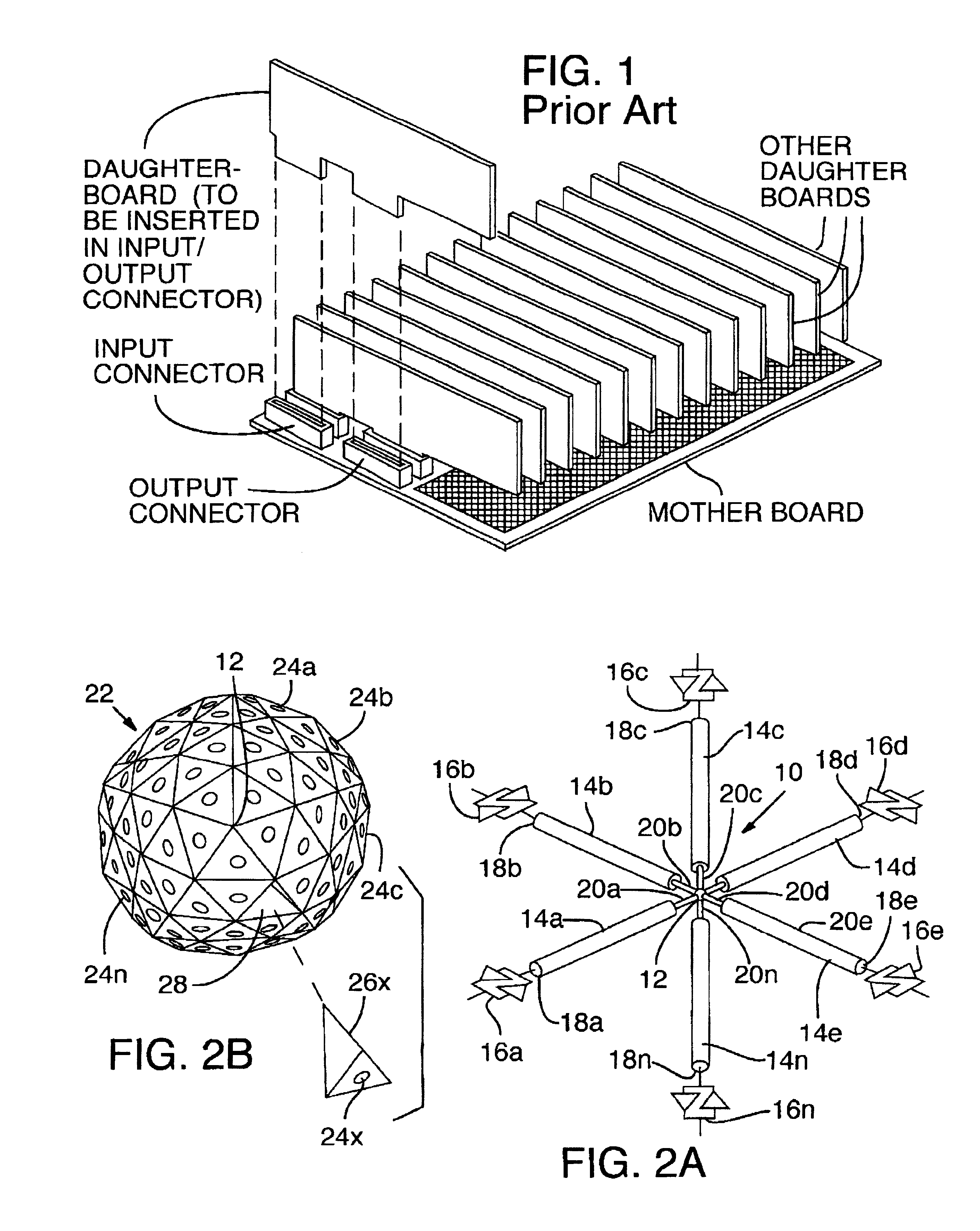
FIG. 1 is an illustration of a typical prior art structure for arranging and connecting a multiplicity of PC boards. A master board, or ‘motherboard’, contains circuitry which controls the interaction between, and operation of, the separate dependent boards, which are called ‘daughterboards’ (for obvious reasons). The daughterboards interface with the motherboard through two rows of multi-conductor sockets shown thereon, one row of which may be used for signal input, and the other of which may be used for signal output from the daughterboards. The wiring interconnecting the various sockets—and the motherboard control circuitry—will be printed on one or more surfaces (sometimes internal) of the motherboard.

It can be seen from FIG. 1 that some signals may have to go from the output elements of the nearest daughterboard to the input elements of the farthest thereof. The physical separation of these elements on this structure can be nearly 8 ins. (20 cm), with perhaps another 0.6 ins. (...


PUM


Abstract

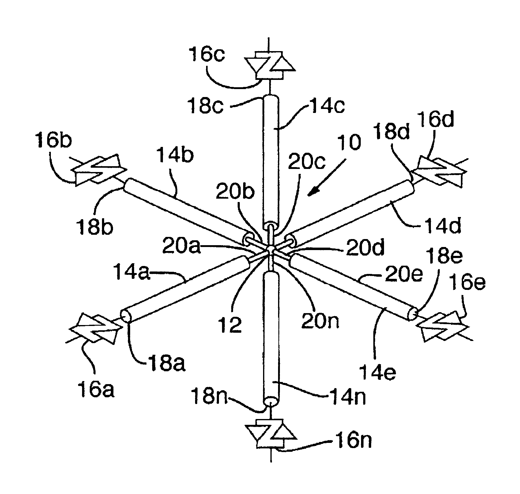
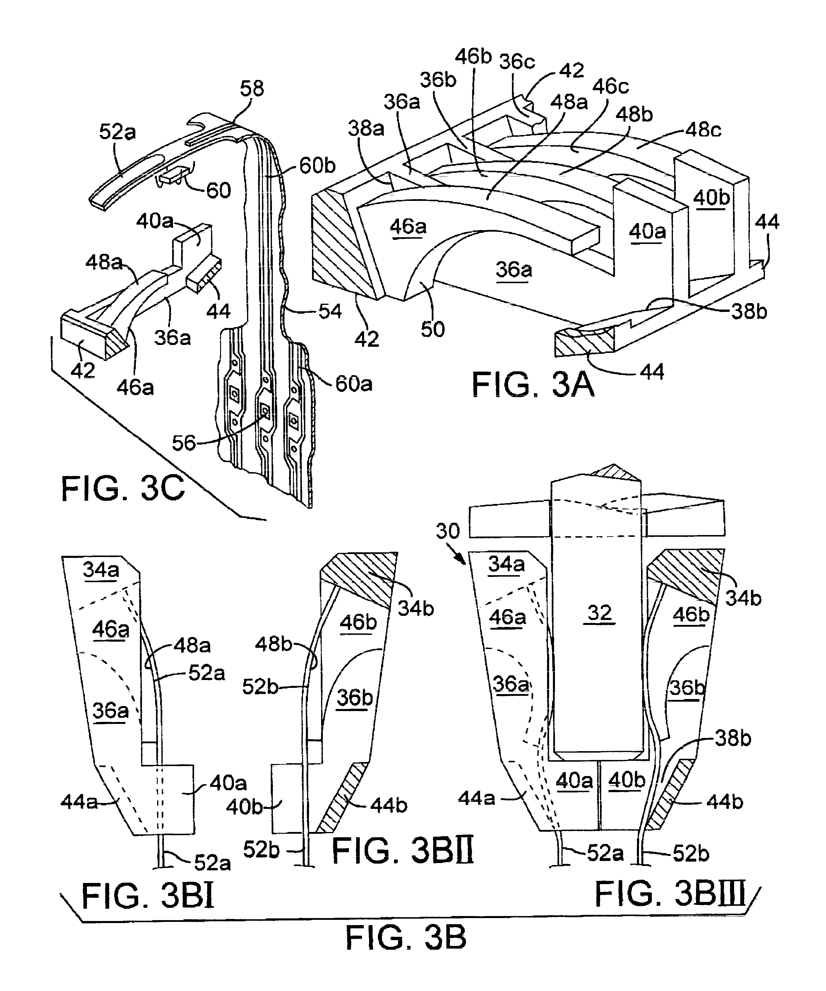
The invention relates to methods and structures for connecting circuits and circuit elements processing electrical signals having very fast transition times, including sub-nanosecond transition times. It includes a connecting structure for connecting a multiplicity of signal lines at a common point to reduce unwanted reflections thereat; a single or multi-conductor female connector for receiving thin elements such as ribbon cable ends, printed circuit (PC) board edges, and the like; a structure for connecting together a multiplicity of ribbon cables terminating in such multi-conductor female connectors, and a further structure for connecting together a multiplicity of such multi-cable connectors to obtain maximum packing thereof, and minimum conductor lengths thereto, to obtain processing rates up to twenty-fold over what is available with present connecting methods and structures.

Description

In general, the invention is a method including a structure, and further structures for connecting electrical elements, for shortening the physical and electrical distances between adjacent electronic elements which process electrical signals having very fast transition times, including sub-nanosecond transition times.In particular, when a multiplicity of signal lines having similar characteristic impedances are connected at a common connection and a signal having said fast transition times is introduced on one of said lines, the structure of the present invention significantly reduces unwanted reflections of said signal on the balance of said lines at said common connection. Also included in the present invention is a connector structure, and a novel arrangement of a multiplicity of said connector structures, for shortening the physical and electrical distances between adjacent printed circuit (hereinafter “PC”) boards mounting integrated circuit (hereinafter “IC”) chips. Further, ...

Claims


Application Information

Patent Timeline
Patent Type & Authority Patents(United States)
IPC IPC(8): H01P5/12H01R13/514H01R13/719H05K7/14
CPCH01P5/12H01R13/514H05K7/1442H01R23/6873H01R13/719H01R13/6473
Inventor COMPTON, PETER M.
Owner HUB TECH INC
Learn More