Memory array with continuous current path through multiple lines

a technology of memory arrays and paths, applied in the direction of digital storage, instruments, semiconductor devices, etc., can solve the problem of minimal improvement of access time, and achieve the effect of increasing density and speeding up data access

Inactive Publication Date: 2005-01-04
SAMSUNG ELECTRONICS CO LTD
View PDF10 Cites 58 Cited by
  • Summary
  • Abstract
  • Description
  • Claims
  • Application Information

AI Technical Summary

Benefits of technology

A memory array according to a particular embodiment of the invention includes a substrate, a plurality of first select-lines disposed in a plurality of planes generally parallel to the substrate, a plurality of second select-lines formed in pillars disposed generally orthogonal to the substrate, a plurality of memory cells coupled to the first select-lines and the

Problems solved by technology

One issue associated with increasing the speed of memory devices is that as the density of memory cells increases within a given mem

Method used


Image

  • Memory array with continuous current path through multiple lines
  • Memory array with continuous current path through multiple lines
  • Memory array with continuous current path through multiple lines

Examples


Embodiment Construction

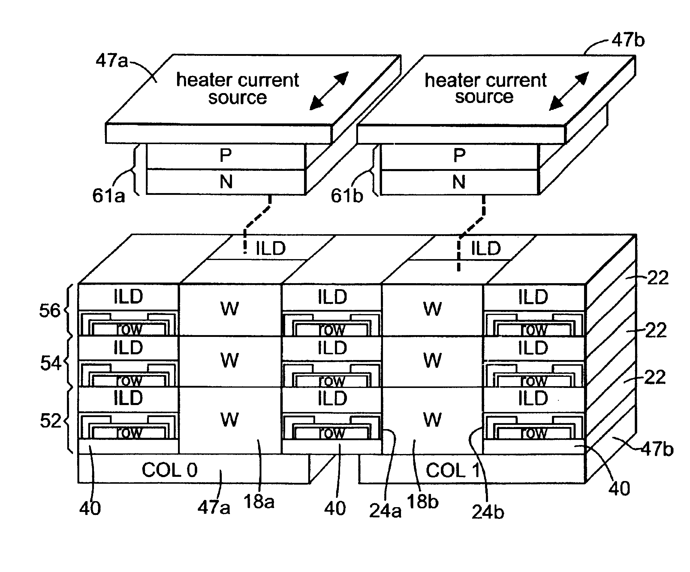
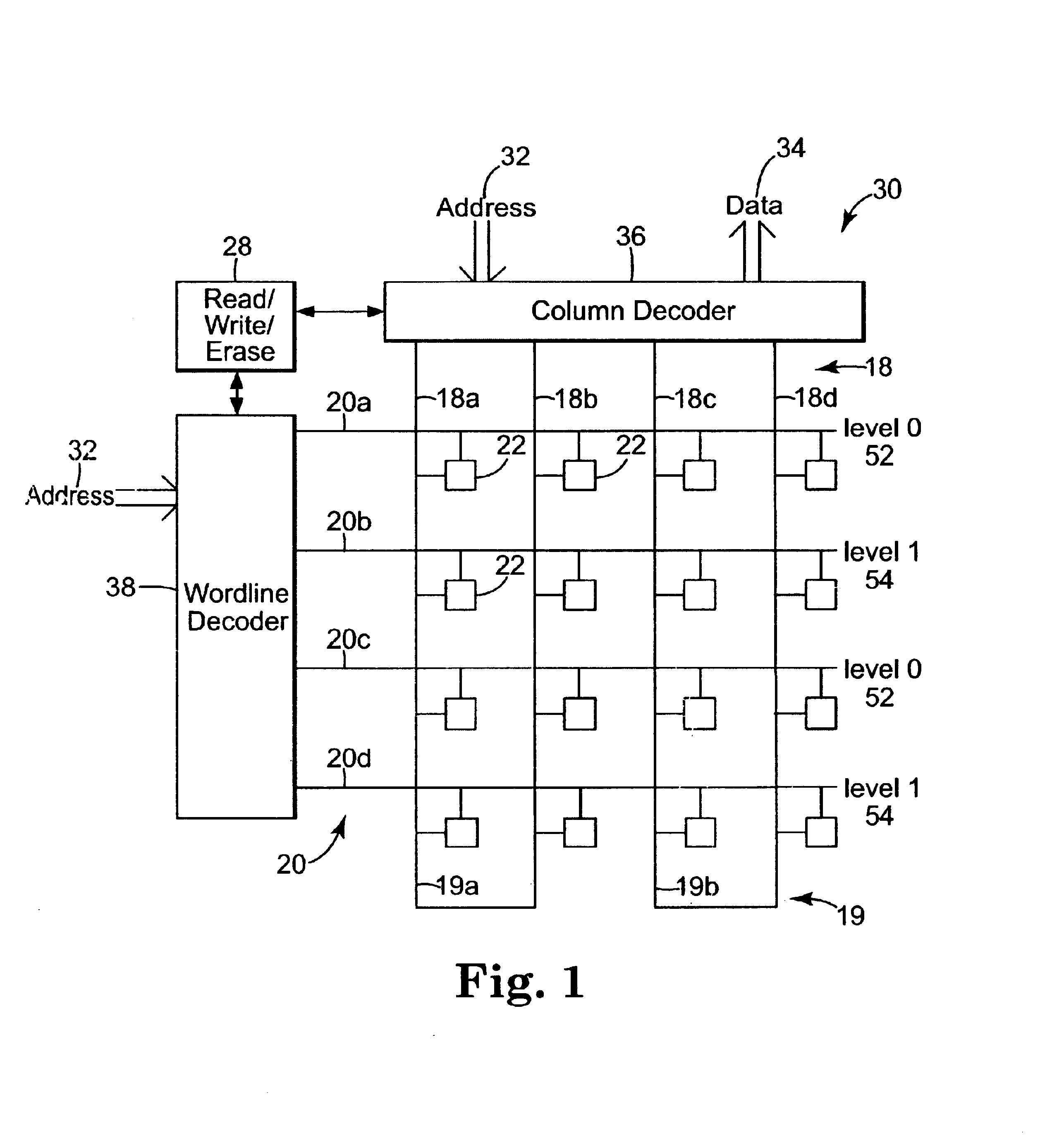
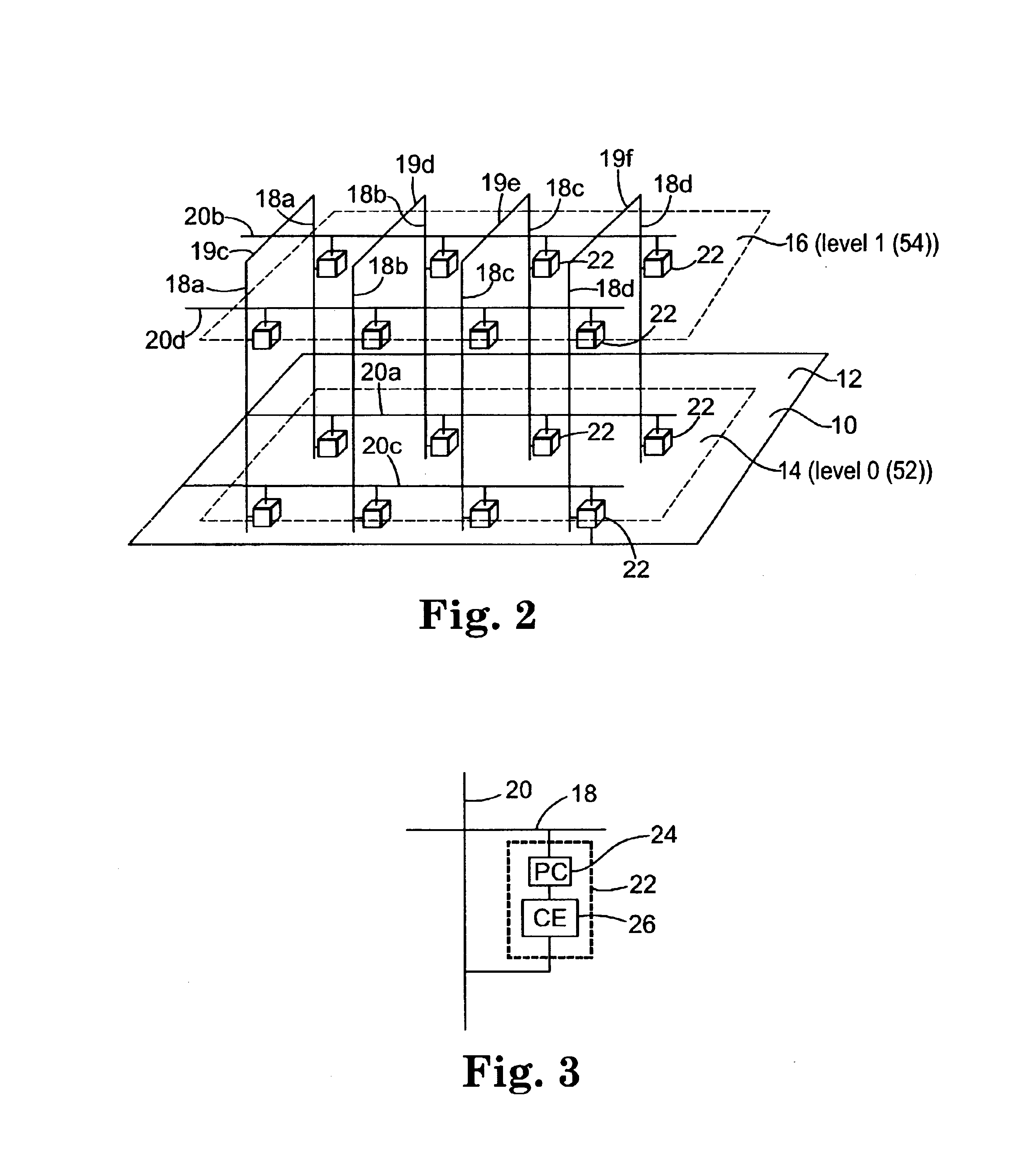
Certain memory architecture embodiments described herein use a vertical pillar to form either the row or column lines used to select a particular memory cell within an array of memory cells. This architecture creates a ‘cubed’ array structure out of a plurality of memory cells that optionally is volumetrically more space-efficient, faster, and easier to manufacture than previous three-dimensional-architectures that simply expand cross-point memory arrays by stacking them. Certain embodiments described herein involve rewritable storage elements, for example phase-change storage elements. Other embodiments involve write-once arrays, also known as one-time programmable (OTP) memory or write-once read-many (WORM) memory. When implementing write-once arrays using vertical pillars as bit-lines (or alternatively word-lines) in a ‘cubic’ (i.e. having three dimensions, although not each necessarily the same length) memory array, a tunnel junction may be formed on the vertical pillar at the i...


PUM


Abstract

A memory array according to a particular embodiment of the invention includes a substrate, a plurality of first select-lines disposed in a plurality of planes generally parallel to the substrate, a plurality of second select-lines formed in pillars disposed generally orthogonal to the substrate, a plurality of memory cells coupled to the first select-lines and the second select-lines, and a current path connection providing a continuous current path through a selected plurality of the pillars to heat the selected pillars and cause at least one memory cell associated with the selected pillars to be reset.

Description

BACKGROUND OF THE INVENTIONPersonal computers, workstations, graphic subsystems of displays, electronic games, and other electrical devices all include memory systems for storing data. An ever-increasing demand exists for larger and faster memory systems. Attributes of memory technologies include data access time (i.e. speed), cost, reliability, size (i.e. density), and electrical power dissipation. Memory technologies include, for example, floppy drives, hard drives, compact disc / digital-video disc (CD / DVD) drives and semiconductor memories. Semiconductor memories include dynamic random access memories (DRAMs), static random access memories (SRAMs), read-only memories (ROMs), programmable read-only memories (PROMs), one-time programmable (OTP) memories, electronically erasable read-only memories (EEPROMs), FLASH memory, and video random access memories (VRAM), for example. While microprocessor-processing power has increased significantly in keeping with Moore's Law, memory devices ...

Claims


Application Information

Patent Timeline
IPC IPC(8): G11C16/02H01L27/24
CPCG11C13/0004H01L27/24G11C2213/71H10B63/22H10B63/845H10B63/20H10N70/821H10N70/8825H10N70/231H10N70/884H10N70/8828H10B63/00
Inventor FRICKE, PETERVANBROCKLIN, ANDREWJACKSON, WARREN
Owner SAMSUNG ELECTRONICS CO LTD
Why Eureka
Try Eureka