Semiconductor manufacturing system and control method thereof

Inactive Publication Date: 2005-01-04
TOKYO ELECTRON LTD
View PDF15 Cites 33 Cited by
  • Summary
  • Abstract
  • Description
  • Claims
  • Application Information

AI Technical Summary

Benefits of technology

It is a general object of the present invention to provide an improved and useful sem

Problems solved by technology

Additionally, since it is not considered in the conventional semiconductor integrated circuit manufacturing apparatus to apply a special treatment when the apparatus malfunctions in the middle of the process and stops for a certain period of time, th

Method used


Image

  • Semiconductor manufacturing system and control method thereof
  • Semiconductor manufacturing system and control method thereof
  • Semiconductor manufacturing system and control method thereof

Examples


Embodiment Construction

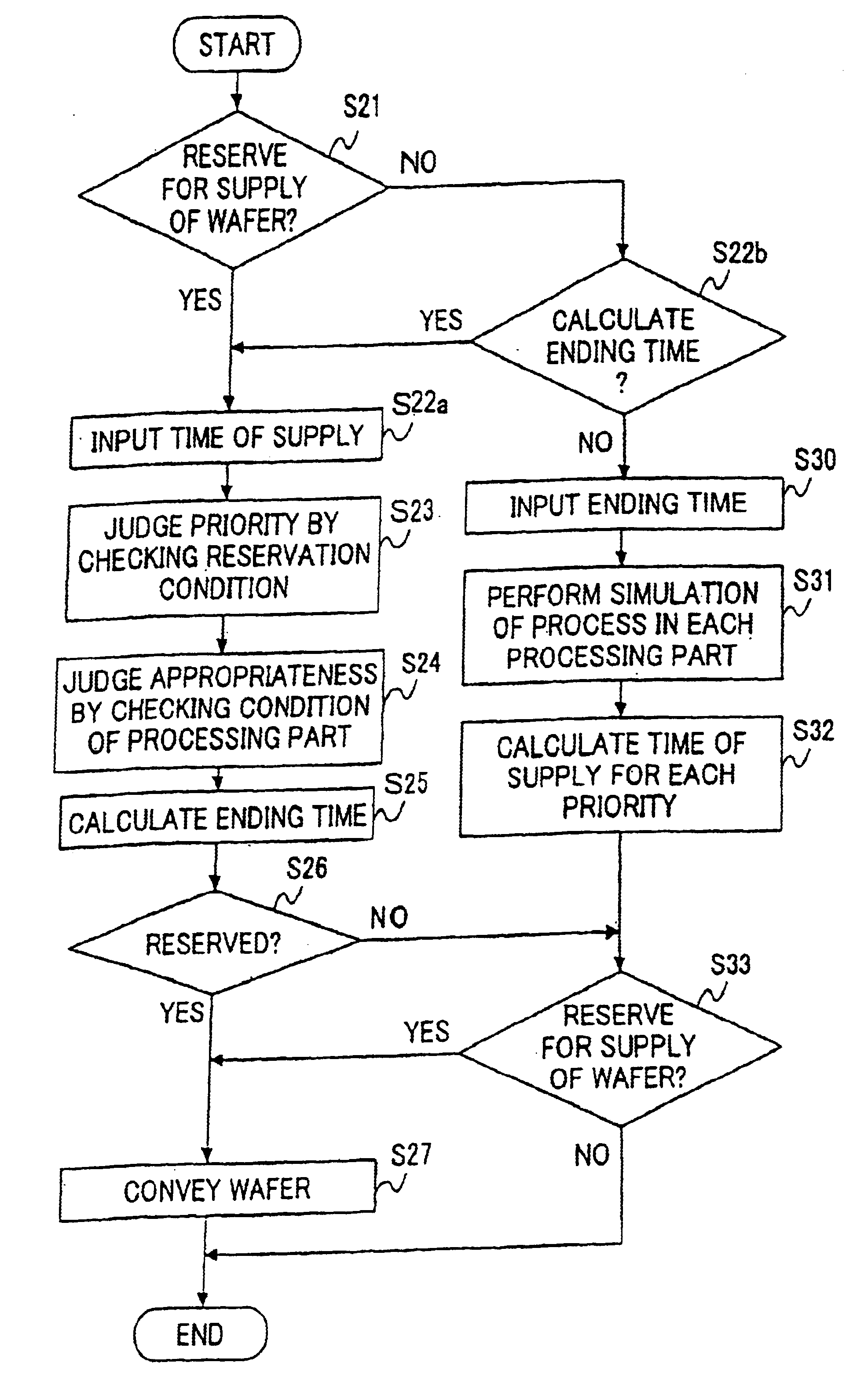
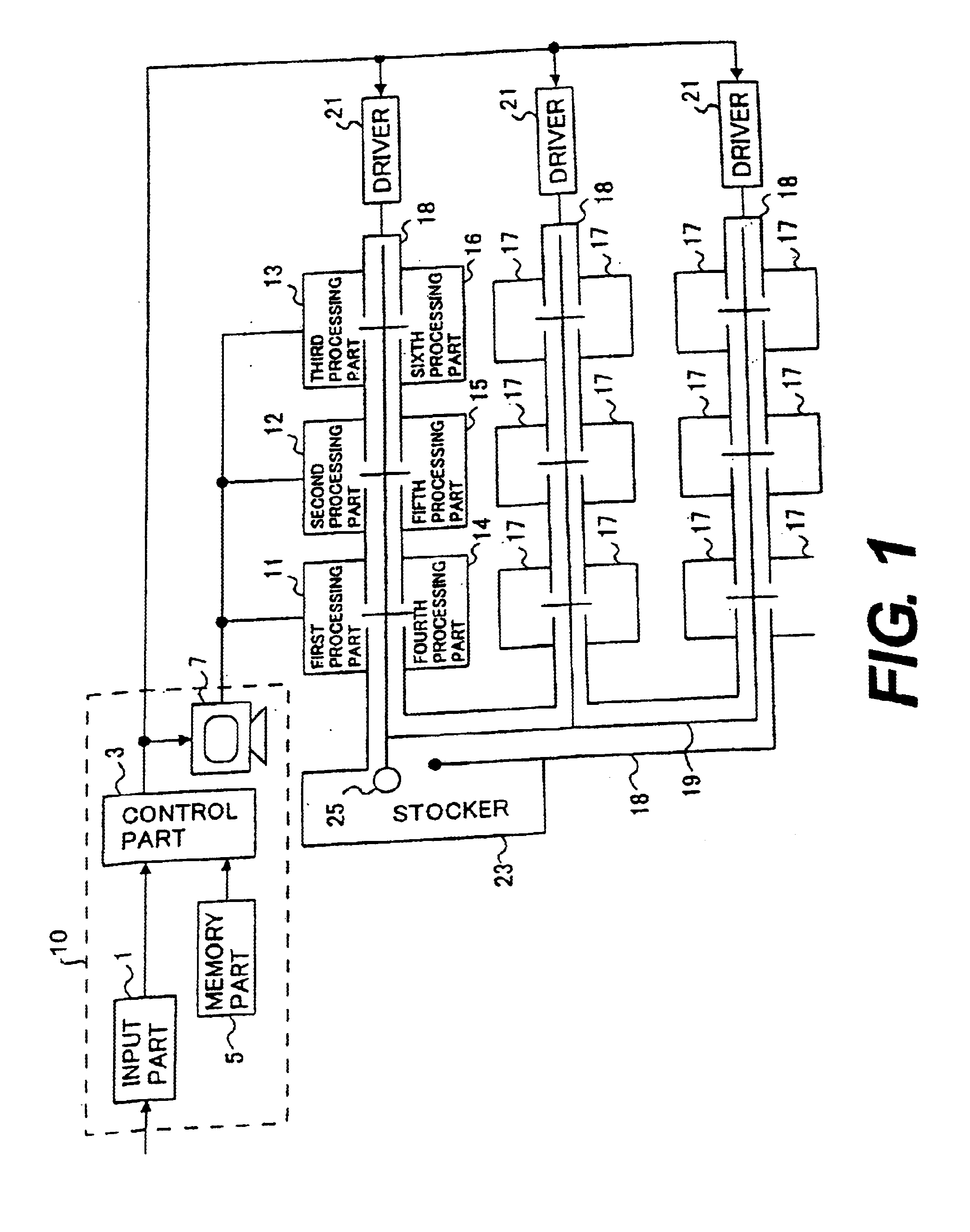
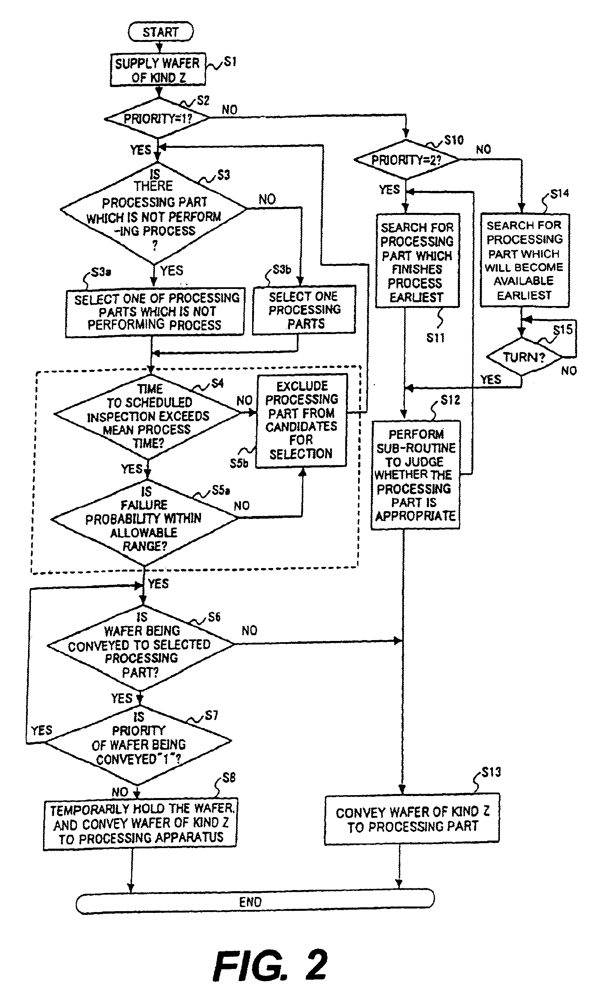
A description will now be given, with reference to the drawings, of an embodiment of the present invention. In the drawings, same parts are given the same reference numerals. Although the semiconductor integrated circuit manufacturing system which manufactures semiconductor integrated circuits on a wafer is explained in detail below, the present invention is applicable also to a system which manufactures a liquid-crystal display panel or the like.

FIG. 1 shows a structure of a semiconductor integrated circuit manufacturing system according to an embodiment of the present invention. As shown in FIG. 1, the semiconductor integrated circuit manufacturing system according to the present embodiment comprises a process control part 10, first to sixth processing parts 11-16, processing parts 17, a conveyance way 18, a conveyance orbit 19, drivers 21 and the stocker 23. The process control part 10 contains the input part 1, the first control part 3, the memory part 5, and the second control ...


PUM


Abstract

In a semiconductor manufacturing system, operations of a plurality of processing apparatuses are controlled so as to efficiently manufacture semiconductor devices. The semiconductor manufacturing system having at least one processing apparatus for applying a process to semiconductor substrates. A memory part (5) stores priority-level data which indicates a priority level of the process to be applied to each of the semiconductor substrates on an individual semiconductor substrate basis. A control part (3, 7) controls the processing apparatus to apply the process to a newly supplied one of the semiconductor substrates by determining an order of processing the newly supplied one of the semiconductor substrates being supplied to the processing apparatus based on a comparison of new priority-level data with the priority-level data stored in the memory part with respect to the semiconductor substrates of which process has been scheduled, the new priority-level data being supplied in response to the newly supplied one of the semiconductor substrates being supplied to the processing apparatus.

Description

This is the National Stage of International Application No. PCT / JP01103846, which was filed in the English language on May 8, 2001, and designated the U.S.TECHNICAL FIELDThe present invention relates to a semiconductor integrated circuit manufacturing system and, more particularly, to a control method of a semiconductor integrated circuit manufacturing system and a computer-readable recording medium, which stores programs for realizing the control method of a semiconductor integrated circuit manufacturing system.BACKGROUND ARTIn a conventional semiconductor integrated circuit, a time spent on each manufacturing process is calculated manually. For example, a time when a wafer is supplied to a process chamber and a time when the process for the wafer is ended are recorded repeatedly, and a time taken for the process is roughly calculated based on the time of supply and the time of ending the process.Additionally, since it is not considered in the conventional semiconductor integrated ...

Claims


Application Information

Patent Timeline
IPC IPC(8): G05B19/418H01L21/02
CPCG05B19/41865G05B2219/32254G05B2219/32256G05B2219/45031G05B2219/32297G05B2219/32349G05B2219/32266Y02P90/02H01L21/00
Inventor KARASAWA, WATARU
Owner TOKYO ELECTRON LTD
Why Eureka
Try Eureka