TFT mask ROM and method for making same

a technology of mask rom and thin film transistor, which is applied in the direction of transistors, solid-state devices, instruments, etc., can solve the problems of increasing the cost of mask rom and less than the optimum cell density

Inactive Publication Date: 2005-01-11
WODEN TECH INC
View PDF149 Cites 294 Cited by
  • Summary
  • Abstract
  • Description
  • Claims
  • Application Information

AI Technical Summary

Problems solved by technology

This cell area is larger than desirable, and leads to a less than optimum cell density, which increases the cost of the mask ROM.

Method used


Image

  • TFT mask ROM and method for making same
  • TFT mask ROM and method for making same
  • TFT mask ROM and method for making same

Examples


Embodiment Construction

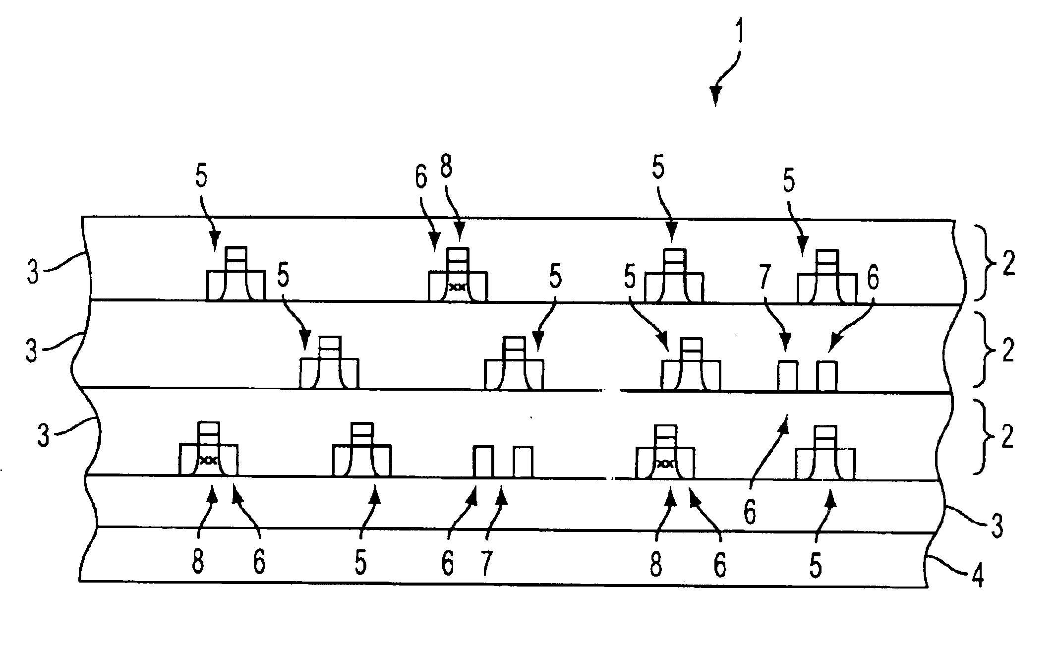
In a preferred embodiment of the present invention, mask ROM density is increased and its cost is decreased by forming a the mask ROM as a monolithic three dimensional array of TFTs. By integrating the array in three dimensions, the effective cell area of the array is reduced to 4F2 / N, where F is the minimum feature size and N is the number of device levels in the array.

FIG. 1 illustrates a monolithic three dimensional TFT mask ROM array 1 according to a preferred embodiment of the present invention. The array comprises a plurality of device levels 2 separated by interlevel insulating layers 3. There may be two or more device levels, such as four to eight device levels 2, separated by one or more interlevel insulating layers 3, such as three to seven insulating layers 3. The device levels 2 alternate with interlevel insulating layers 3. The array 1 is preferably formed over a substrate 4.

Each device level 2 contains a first set of enabled TFTs 5 and a second set of partially or tota...


PUM


Abstract

There is provided a monolithic three dimensional TFT mask ROM array. The array includes a plurality of device levels. Each of the plurality of device levels contains a first set of enabled TFTs and a second set of partially or totally disabled TFTs.

Description

FIELD OF THE INVENTIONThe present invention is directed generally to semiconductor devices and methods of fabrication and more particularly to a thin film transistor (TFT) mask ROM and method of fabrication.BACKGROUND OF THE INVENTIONThin film transistors (TFTs) are utilized in various devices, such as a liquid crystal displays, static random access memories and in nonvolatile memories. U.S. Pat. Nos. 5,572,046 and 5,383,149 also suggest using TFTs in a mask read only memory (mask ROM or MROM). Conventional TFTs have a structure that is similar to conventional bulk metal oxide semiconductor field effect transistors (MOSFETs), except that TFTs are formed in a semiconductor layer that is located above an insulating substrate, such as a glass substrate, or above a semiconductor substrate that is covered by an insulating layer.The mask ROM derives its name from the fact that this nonvolatile memory is programmed or written using a custom mask during fabrication. In a conventional mask R...

Claims


Application Information

Patent Timeline
Patent Type & Authority Patents(United States)
IPC IPC(8): H01L27/112H01L27/06H01L27/12G11C17/12H01L21/336H01L21/77H01L21/822H01L21/8244H01L21/8246H01L21/8247H01L21/84H01L27/105H01L27/11H01L27/115
CPCG11C17/12H01L29/66825H01L21/84H01L27/0688H01L27/105H01L27/11H01L27/1108H01L27/1116H01L27/112H01L27/1126H01L27/1128H01L27/11286H01L27/11293H01L27/115H01L27/11517H01L27/11521H01L27/11526H01L27/11551H01L27/11568H01L27/11578H01L27/1203H01L27/1214H01L21/8221H01L27/11803H10B10/125H10B10/18H10B10/00H10B20/383H10B20/50H10B20/60H10B20/65H10B20/00H10B41/00H10B41/40H10B41/20H10B43/20H10B43/30H10B69/00H10B41/30
Inventor WALKER, ANDREW J.PETTI, CHRISTOPHER
Owner WODEN TECH INC
Why Eureka
Try Eureka