Radio frequency data communication device in CMOS process

a technology of radio frequency data and communication device, applied in the field of radio frequency identification (rfid) chips, can solve the problem of high cost of current available rfid chips configured with external batteries, and achieve the effect of reducing cos

Inactive Publication Date: 2005-01-11
XUESHAN TECH INC
View PDF10 Cites 106 Cited by
  • Summary
  • Abstract
  • Description
  • Claims
  • Application Information

AI Technical Summary

Benefits of technology

[0009]The present invention is directed to a RF data communication device that can be manufactured in the mature ...

Problems solved by technology

However, current available RFID chips co...

Method used


Image

  • Radio frequency data communication device in CMOS process
  • Radio frequency data communication device in CMOS process
  • Radio frequency data communication device in CMOS process

Examples


Embodiment Construction

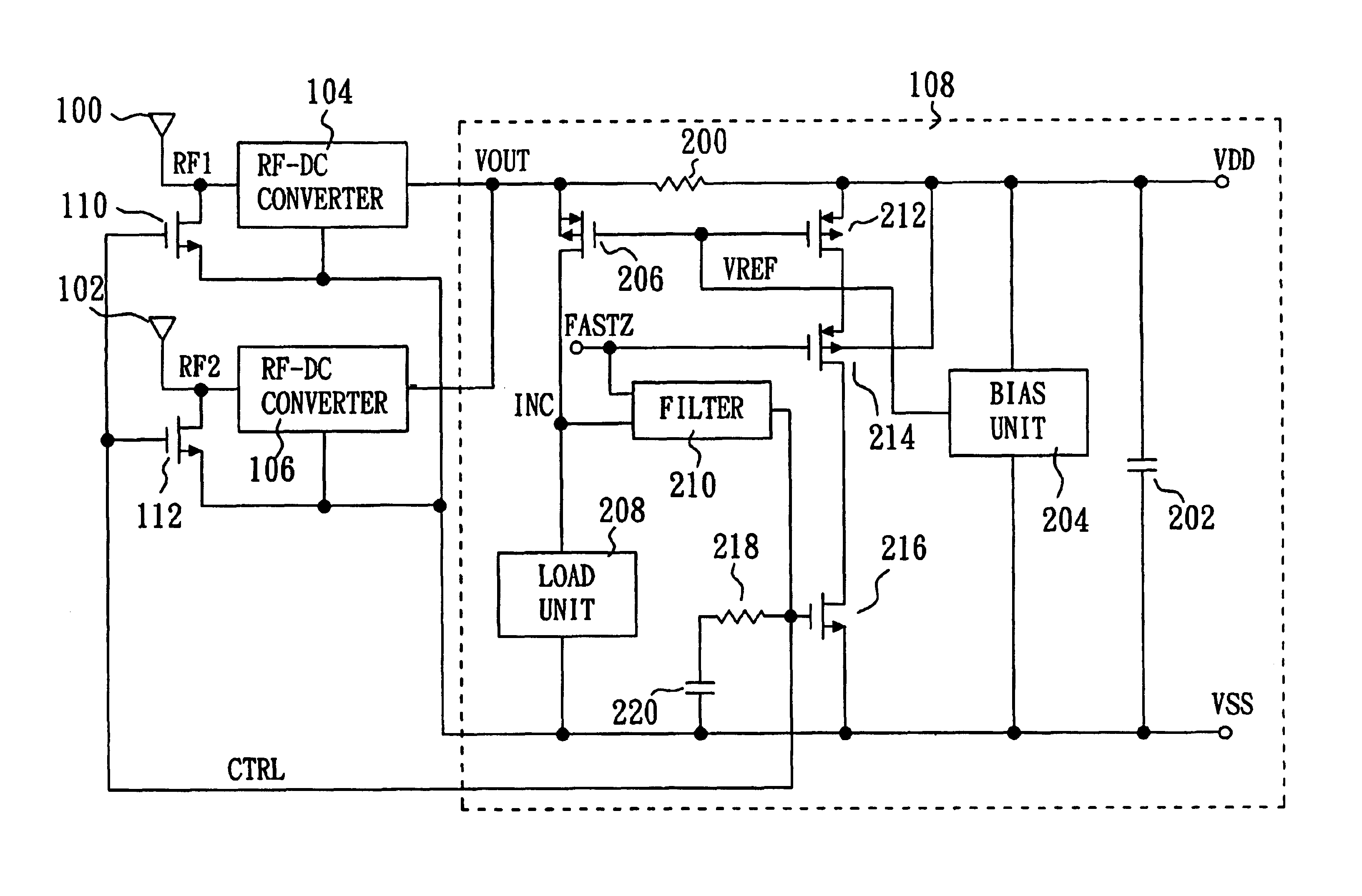
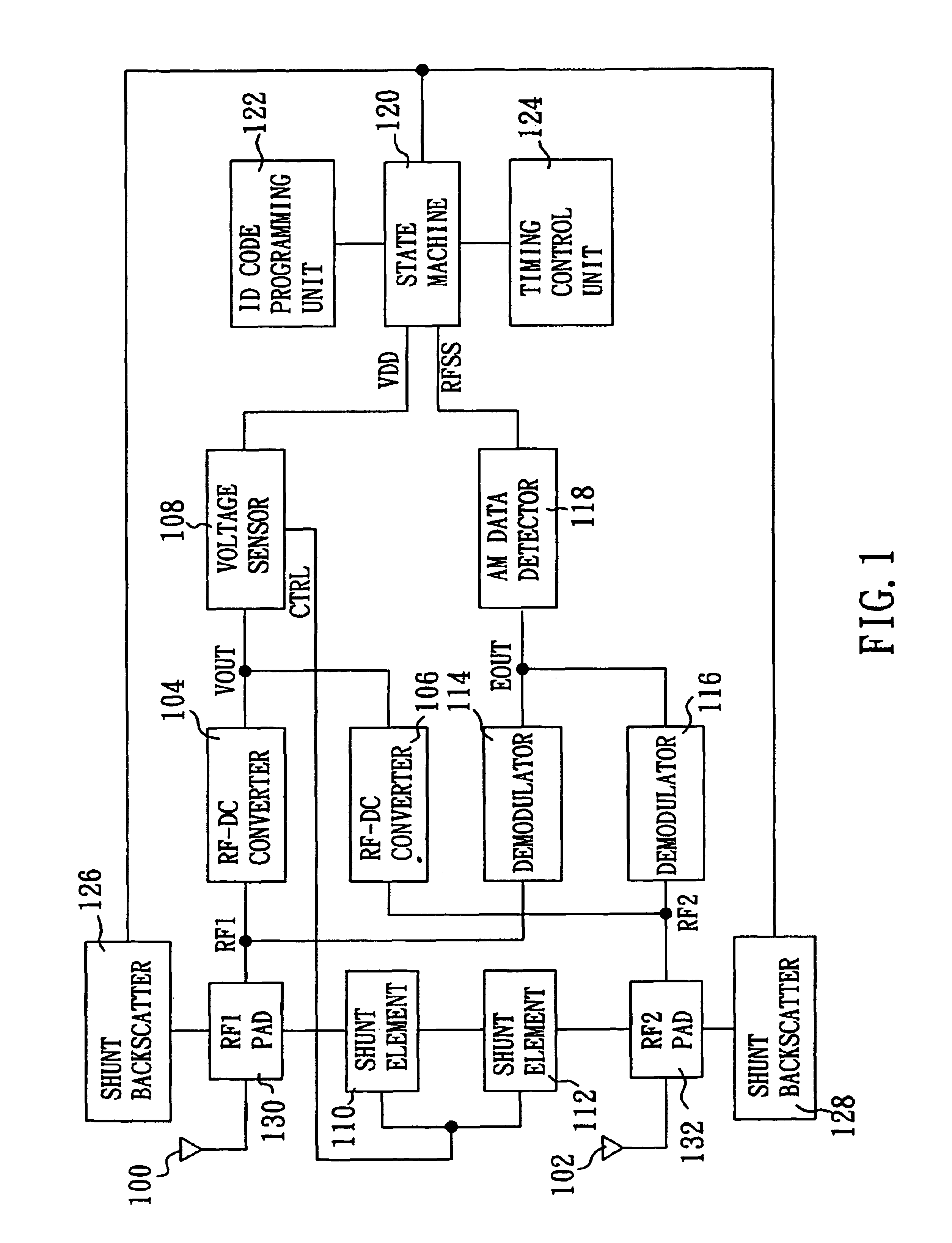
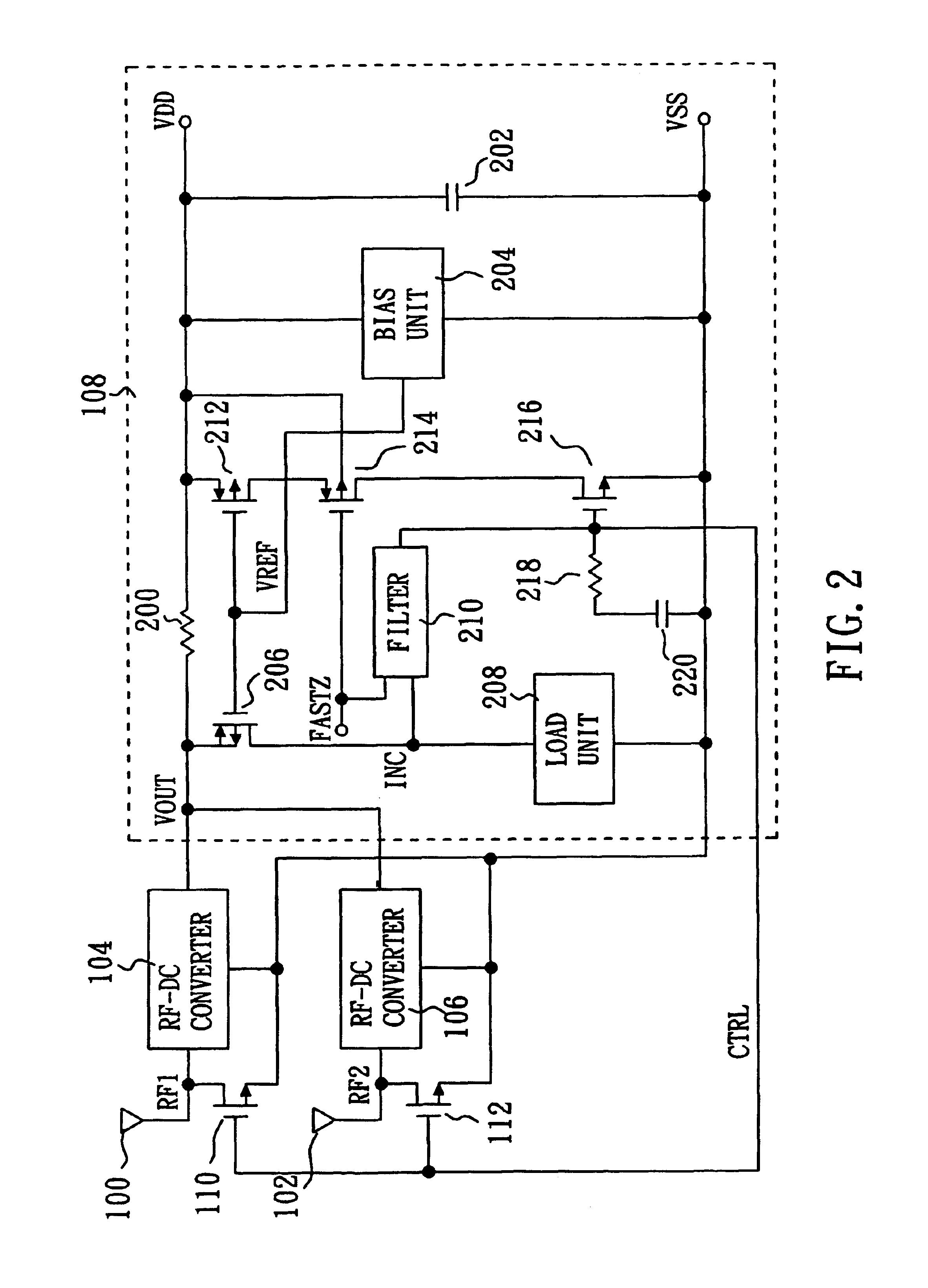
[0023]Referring to FIG. 1, a block diagram of a passive RFID chip in accordance with the present invention is schematically illustrated. The term “passive” means that the RFID chip is provided with on-chip RF-DC converters for generating the required electrical power for the chip from incoming RF energy. The passive RFID chip of the present invention is provided with a first pad 130 and a second pad 132 operatively connected to a first antenna 100 and a second antenna 102 for receiving RF signals RF1 and RF2, respectively. The first antenna 100 and the second antenna 102 are so arranged that the average gain over all orientations is increased with respect to each antenna separately. Preferably, dipole antenna designs which the first antenna 100 would be oriented at a 90 degree angle with respect to the second antenna 102 on the same plane.

[0024]The passive RFID chip of the present invention can be categorized to an analog portion and a digital portion. As shown in FIG. 1, the analog...


PUM


Abstract

The present invention provides a passive RFID chip with on-chip charge pumps for generating electrical power for the chip from radio frequencies. The passive RFID chip comprises an analog portion and a digital portion. The analog portion primarily comprises a voltage sensor and an AM data detector. The digital portion comprises a state machine digital logic controller. Incoming RF signals enter the chip via external antennas. The RF signals are converted into regulated DC signals by RF-DC converters with the voltage sensor. The RF-DC converters provide power for all the on-chip components and hence the chip does not require external power supply. The incoming RF signals are demodulated by demodulators and enter the AM data detector where the envelope transitions are detected. A voltage alarm is provided to ensure the voltage level does not drop below an operational level of the chip. The logic signals and programming data are controlled by the state machine digital logic controller and the timing signals are provided by an on-chip oscillator.

Description

CROSS-REFERENCE TO RELATED APPLICATION[0002]The present application claims the priority benefits of U.S. provisional application entitled “RADIO FREQUENCY DATA COMMUNICATION DEVICE IN CMOS PROCESS” filed on Apr. 9, 2002 Ser. No. 60 / 371,363. All disclosures of this application are incorporated herein by reference.BACKGROUND OF THE INVENTION[0003]1. Field of the Invention[0004]The present invention generally relates to a radio frequency identification (RFID) chip, and more particularly, to an RFID chip using CMOS technology.[0005]2. Description of Related Arts[0006]In goods-related or services-related industries, it is necessary to inventory the item stock every while. Conventionally, manual labors have been employed to count the items located on the shelf, and those are otherwise located in the store or warehouse for a long time. For the purpose of easing off such time-consuming and labor-intensive jobs, a technology known as radio frequency identification (RFID) is provided to have ...

Claims


Application Information

Patent Timeline
IPC IPC(8): G06K19/07G11C5/14H04B1/00
CPCG06K19/0713G06K19/0723H04B7/086H04B5/0062G11C5/142Y02D30/70
Inventor SMITH, STERLINGYUNG, HENRY TIN-HANG
Owner XUESHAN TECH INC
Why Eureka
Try Eureka