Method and circuit for measuring on-chip, cycle-to-cycle clock jitter

a technology of cycle-to-cycle clock jitter and measurement method, which is applied in the direction of frequency measurement arrangement, frequency to phase shift conversion, instruments, etc., can solve the problems of difficult testing of the jitter performance of the microprocessor, cycle-to-cycle jitter may occur, and the difficulty of clock distribution

Inactive Publication Date: 2005-01-11
HEWLETT-PACKARD ENTERPRISE DEV LP
View PDF6 Cites 54 Cited by
  • Summary
  • Abstract
  • Description
  • Claims
  • Application Information

AI Technical Summary

Problems solved by technology

As clock speeds exceed 2 GHz and die size exceeds 400 square millimeters, clock distribution may become more difficult.
Cycle-to cycle jitter may occur, among other things, due to temperature variation or changes in on-chip voltages.
Measuring the jitter performance of microprocessors can be a difficult testing

Method used


Image

  • Method and circuit for measuring on-chip, cycle-to-cycle clock jitter
  • Method and circuit for measuring on-chip, cycle-to-cycle clock jitter
  • Method and circuit for measuring on-chip, cycle-to-cycle clock jitter

Examples


Embodiment Construction

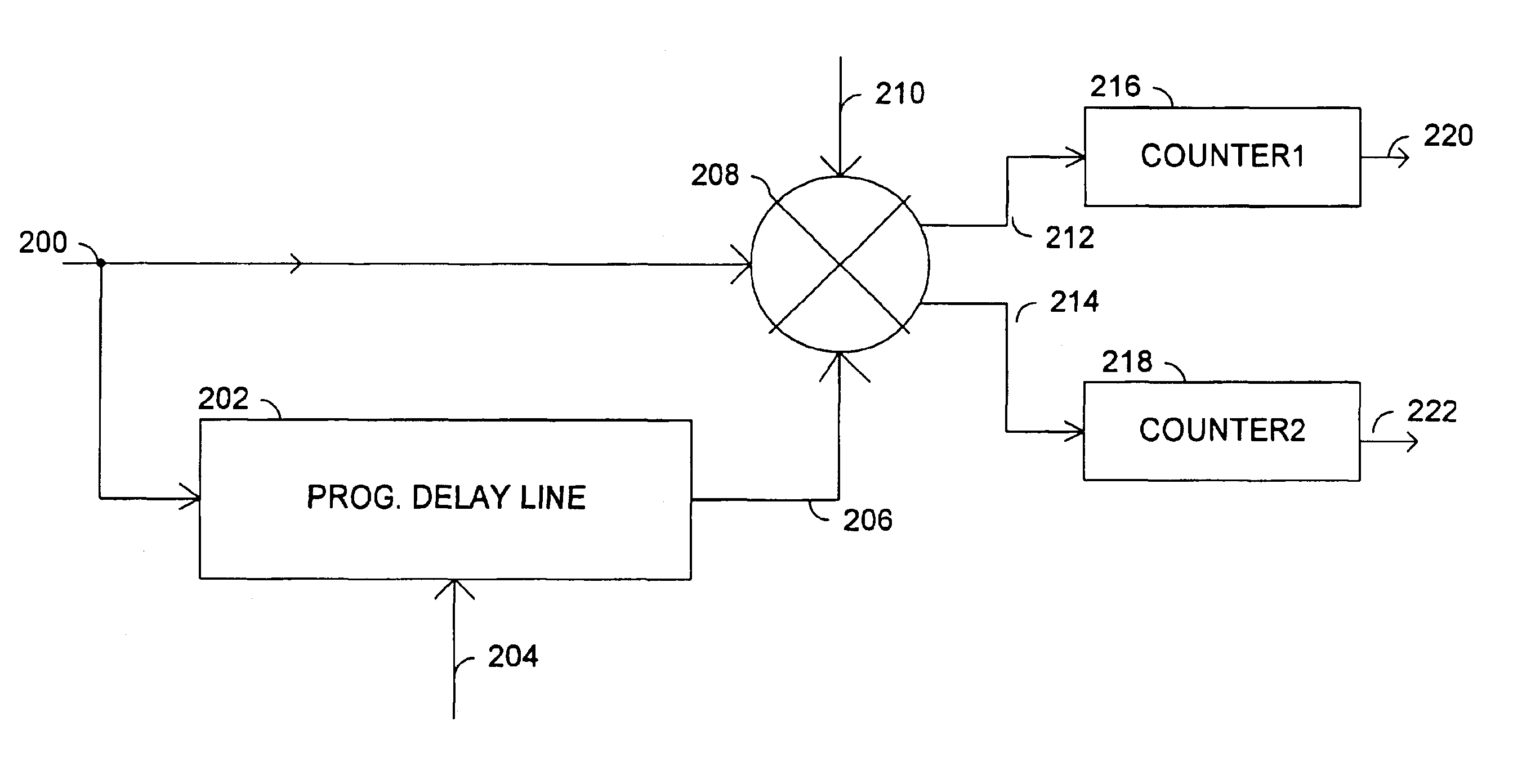
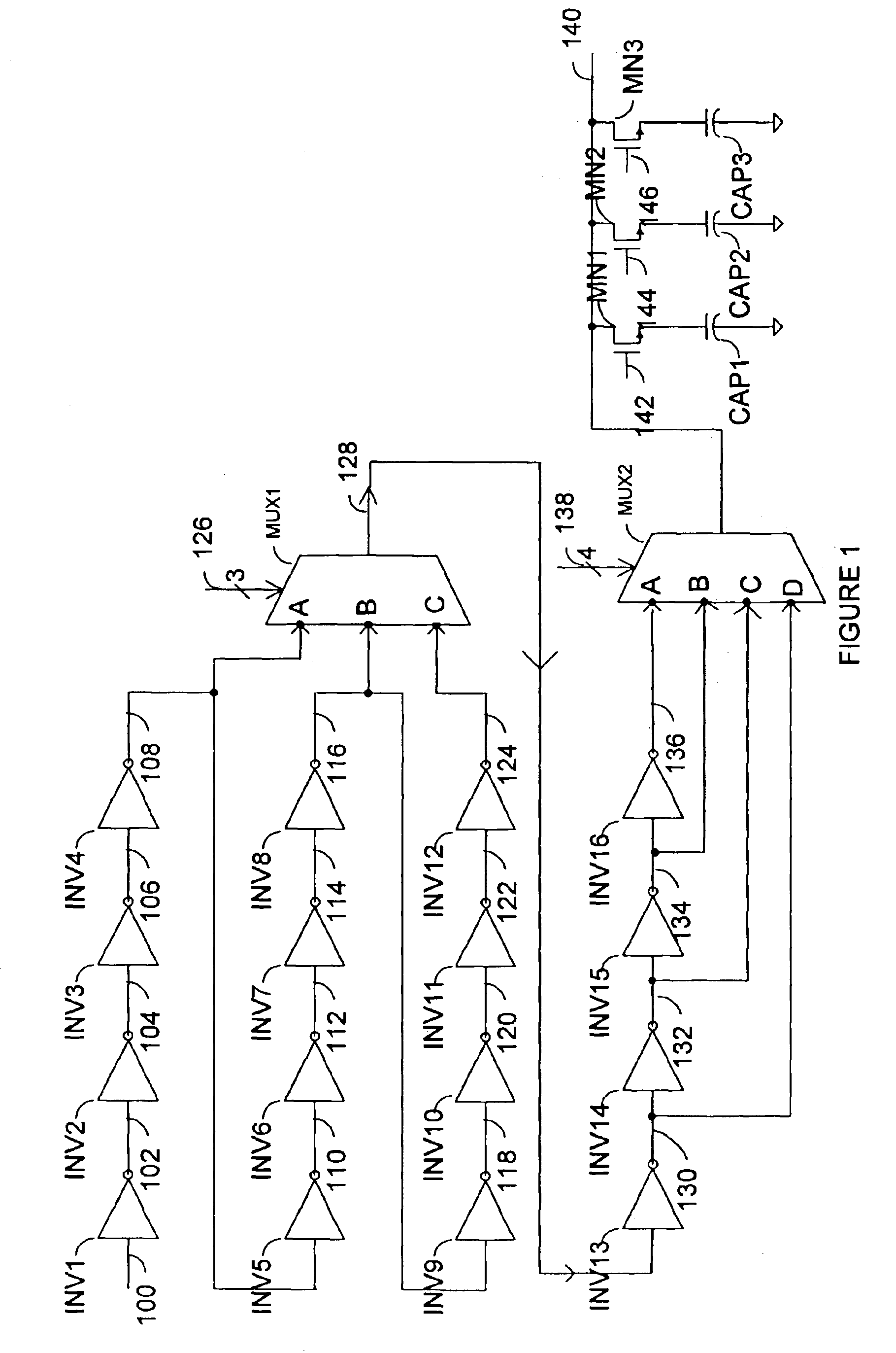
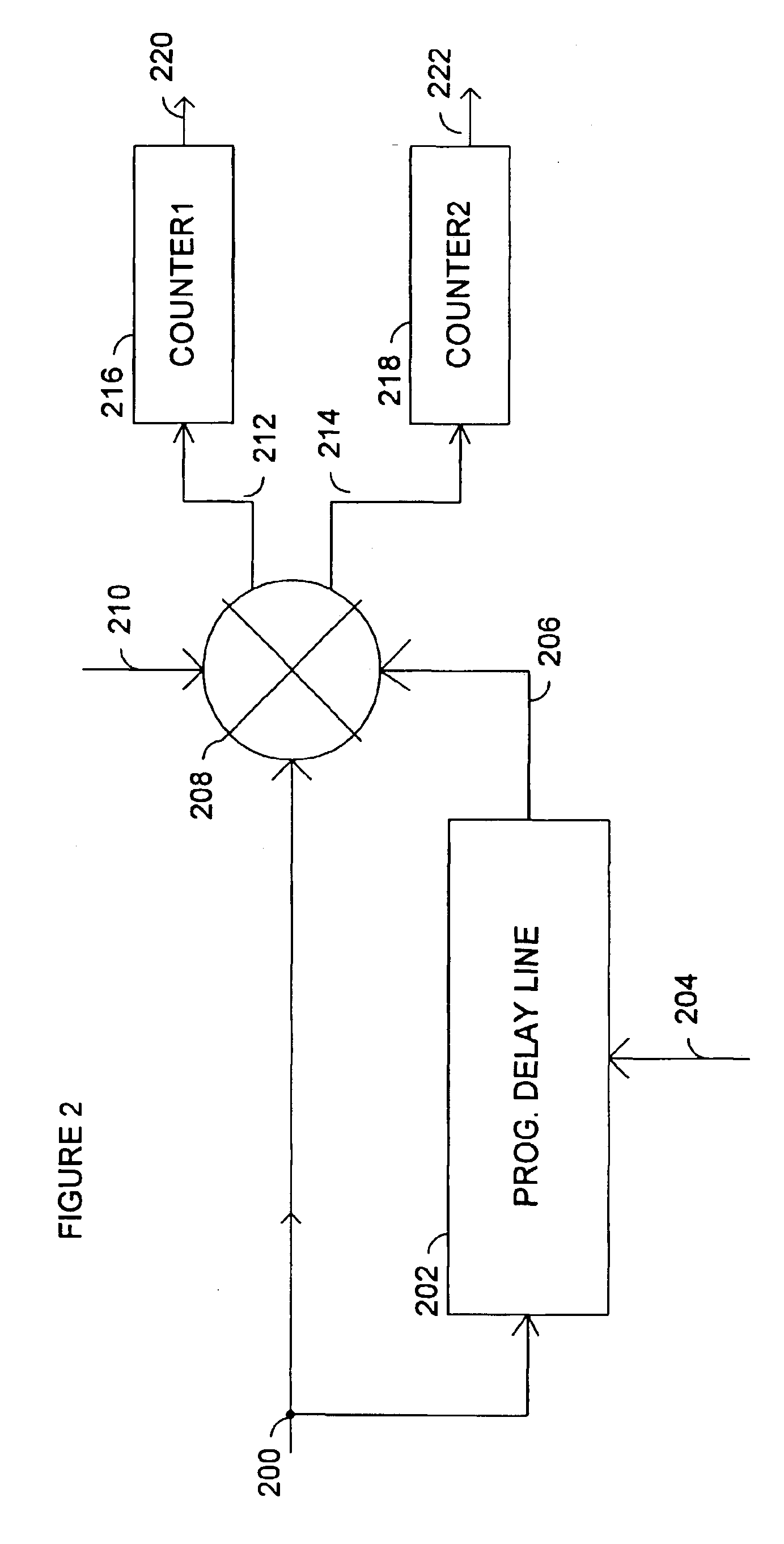
FIG. 1 is a schematic drawing of a programmable delay line. The input, 100, to the programmable delay line is connected to the input of inverter INV1. The output, 102, of inverter INV1 is connected to the input, 102, of inverter INV2. The output, 104, of inverter INV2 is connected to the input, 104, of inverter INV3. The output, 106, of inverter INV3 is connected to the input, 106, of inverter INV4. The output, 108, of inverter INV4 is connected to the input, 106, of inverter INV5 and input A of MUX1. The output, 110, of inverter INV5 is connected to the input, 110, of inverter INV6. The output, 112, of inverter INV6 is connected to the input, 112, of inverter INV7. The output, 114, of inverter INV7 is connected to the input, 114, of inverter INV8. The output, 116, of inverter INV8 is connected to the input, 116, of inverter INV9 and input B of MUX1. The output, 118, of inverter INV9 is connected to the input, 118, of inverter INV10. The output, 120, of inverter INV10 is connected t...


PUM


Abstract

The invention provides a method and circuit for measuring on-chip, cycle-to-cycle, jitter. Copies of a circuit comprising a programmable delay line, a programmable phase comparator, and two counters are placed at different locations on an IC near a clock signal. The programmable delay line creates a clock signal that is delayed by one clock cycle. This delayed clock signal is compared in time to the original clock signal by the programmable phase comparator. If the difference in time between the delayed clock signal and the clock signal is greater than the dead time, the first counter is triggered. If the difference in time is negative and the absolute value is greater than the dead time, the second counter is triggered. A statistical distribution, based on the values of the counters, is created. This distribution is used to predict on-chip, cycle-to-cycle jitter.

Description

FIELD OF THE INVENTIONThis invention relates generally to clocking circuits on integrated electronic circuits. More particularly, this invention relates to measuring on-chip, cycle-to-cycle clock jitter.BACKGROUND OF THE INVENTIONA microprocessor used in many large computer systems may include memory elements, combinational logic, and a clocking system. The memory elements may be arranged in sets, sometimes called registers that may correspond to the word size used in a computer system. Between at least some sets of memory elements are combinational logic circuits. At the end of a clock cycle, which is also the beginning of the next clock cycle, data on the output of the combinational logic circuitry is stored in a first set of memory elements. This data appears on the output of the set of memory elements, and therefore on the input of other combinational logic circuitry. The other logic circuitry performs the designed logic function on the data, and at the end of the clock cycle th...

Claims


Application Information

Patent Timeline
IPC IPC(8): G01R25/00G01R31/28G01R31/317
CPCG01R25/005G01R31/31725G01R31/31709
Inventor FETZER, ERIC S.
Owner HEWLETT-PACKARD ENTERPRISE DEV LP
Why Eureka
Try Eureka