Semiconductor device

Inactive Publication Date: 2009-06-11
KK TOSHIBA
View PDF7 Cites 36 Cited by
  • Summary
  • Abstract
  • Description
  • Claims
  • Application Information

AI Technical Summary

Benefits of technology

[0009]According to an aspect of the invention, there is provided a semiconductor device including: a digital control circuit configured to supply two semiconductor switching elements connected in series in a switching power supply circuit with a pulse signal for turning on/off the semiconductor switching elements; and a dead time setting circuit configured to set a dead time in which the two semiconductor switching elements are both turned off, the dead time setting circuit including: a delay generation circuit including a plurality of delay elements connected in series and having mutually different delay values; and a delay adjustment circuit configured to adjust the delay values of the delay generation circuit so that a setting value of the dead time is determined on basis of correlation betwee

Problems solved by technology

However, in practice, due to variations in switching elements, this method cannot optimize the dead time for all the elements.
Currently, it is difficult to exactly divide one clock cycle into

Method used


Image

  • Semiconductor device
  • Semiconductor device
  • Semiconductor device

Examples


Embodiment Construction

[0017]An embodiment of the invention will now be described with reference to the drawings.

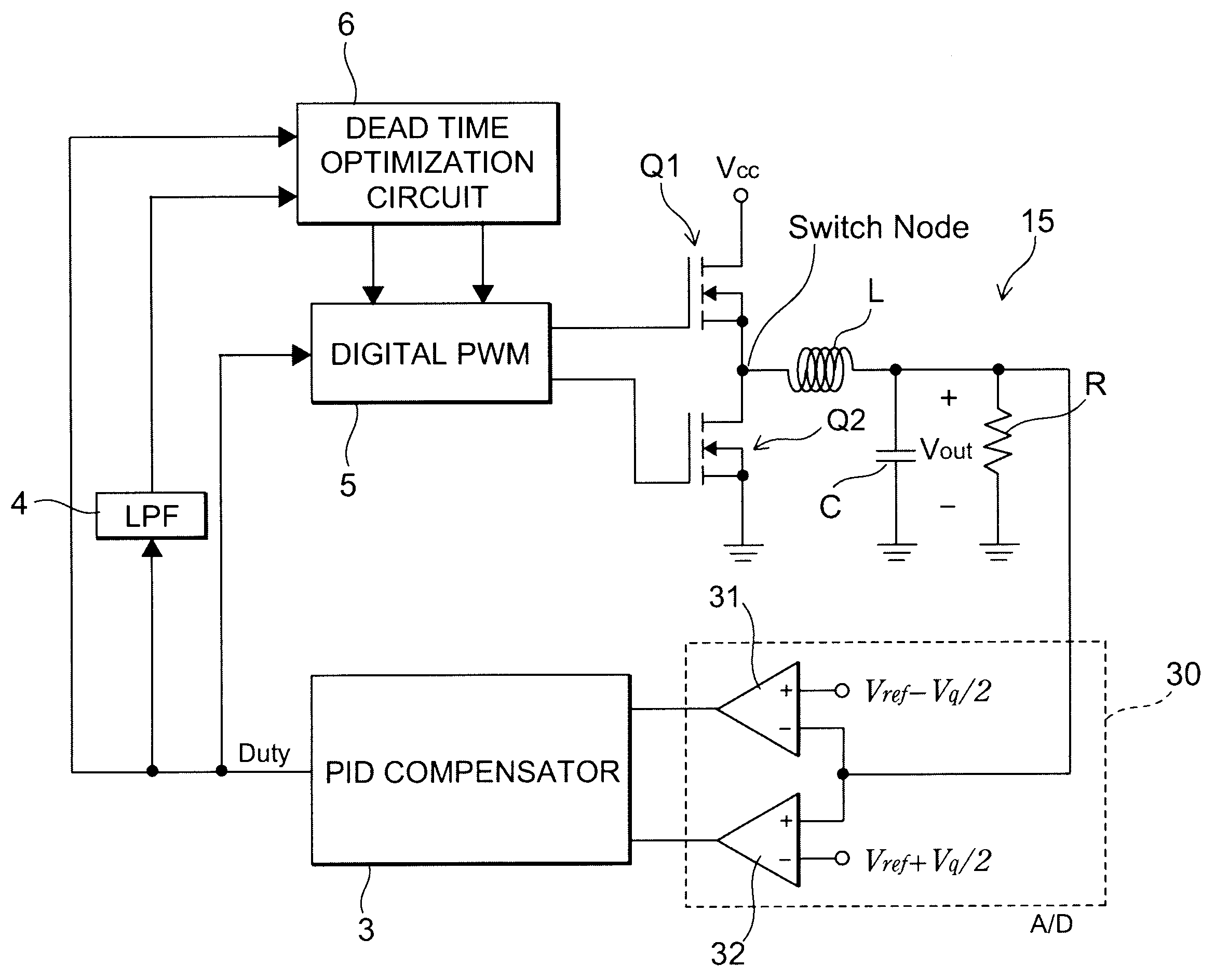
[0018]A semiconductor device according to the embodiment of the invention illustratively includes, in the circuit shown in FIG. 1, switching elements Q1 and Q2, an A / D conversion circuit 30, a PID (proportional-integral-derivative) compensator 3, a low-pass filter 4, a digital control circuit 5, and a dead time setting circuit 6, which are formed on a semiconductor substrate and integrated into one chip.

[0019]The circuit shown in FIG. 1 is a DC-DC converter, broadly divided into a switching power supply circuit 15 including the switching elements Q1 and Q2, an inductor L, a capacitor C, and a load R, and a control circuit for controlling the operation of this switching power supply circuit 15.

[0020]This DC-DC converter is a step-down DC-DC converter (buck converter) for producing an (average) output voltage Vout lower than the input voltage Vcc by alternately turning on / off the high-side switch...


PUM


Abstract

A semiconductor device includes: a digital control circuit configured to supply two semiconductor switching elements connected in series in a switching power supply circuit with a pulse signal for turning on/off the semiconductor switching elements; and a dead time setting circuit configured to set a dead time in which the two semiconductor switching elements are both turned off. The dead time setting circuit includes: a delay generation circuit including a plurality of delay elements connected in series and having mutually different delay values; and a delay adjustment circuit configured to adjust the delay values of the delay generation circuit so that a setting value of the dead time is determined on basis of correlation between the dead time and the duty cycle of the pulse signal.

Description

CROSS-REFERENCE TO RELATED APPLICATIONS[0001]This application is based upon and claims the benefit of priority from the prior Japanese Patent Application No.2007-314551, filed on Dec. 5, 2007; the entire contents of which are incorporated herein by reference.BACKGROUND OF THE INVENTION[0002]1. Field of the Invention[0003]This invention relates to a semiconductor device, and more particularly to a semiconductor device including a circuit in which a semiconductor switching element is digitally turned on / off to produce a desired output.[0004]2. Background Art[0005]In a switching power supply such as a DC-DC converter including a high-side and low-side switching element (power transistor) which are alternately turned on / off by a PWM (pulse width modulation) signal, a dead time for allowing both the power transistors to be turned off is provided to avoid a shoot-through current due to simultaneous turn-on of the power transistors.[0006]The dead time affects the efficiency of the DC-DC co...

Claims


Application Information

Patent Timeline
IPC IPC(8): G05F1/10
CPCH02M1/38Y02B70/1466H02M3/1588H02M3/157Y02B70/10
Inventor NAKA, TOSHIYUKI
Owner KK TOSHIBA
Why Eureka
Try Eureka