Two transistor NOR device

a technology of two transistors and transistors, applied in logic circuits, logic functions, pulse techniques, etc., can solve problems such as the difficulty of conventional mosfets scaling below 50 nm fabrication processing

Inactive Publication Date: 2005-01-11
GLOBALFOUNDRIES U S INC
View PDF7 Cites 13 Cited by
  • Summary
  • Abstract
  • Description
  • Claims
  • Application Information

AI Technical Summary

Problems solved by technology

Conventional MOSFETs have difficulty scaling below 50 nm fabrication processing.

Method used


Image

  • Two transistor NOR device
  • Two transistor NOR device
  • Two transistor NOR device

Examples


Embodiment Construction

The following detailed description of the invention refers to the accompanying drawing. The same reference numbers may be used in different drawings to identify the same or similar elements. Also, the following detailed description does not limit the invention. Instead, the scope of the invention is defined by the appended claims and equivalents.

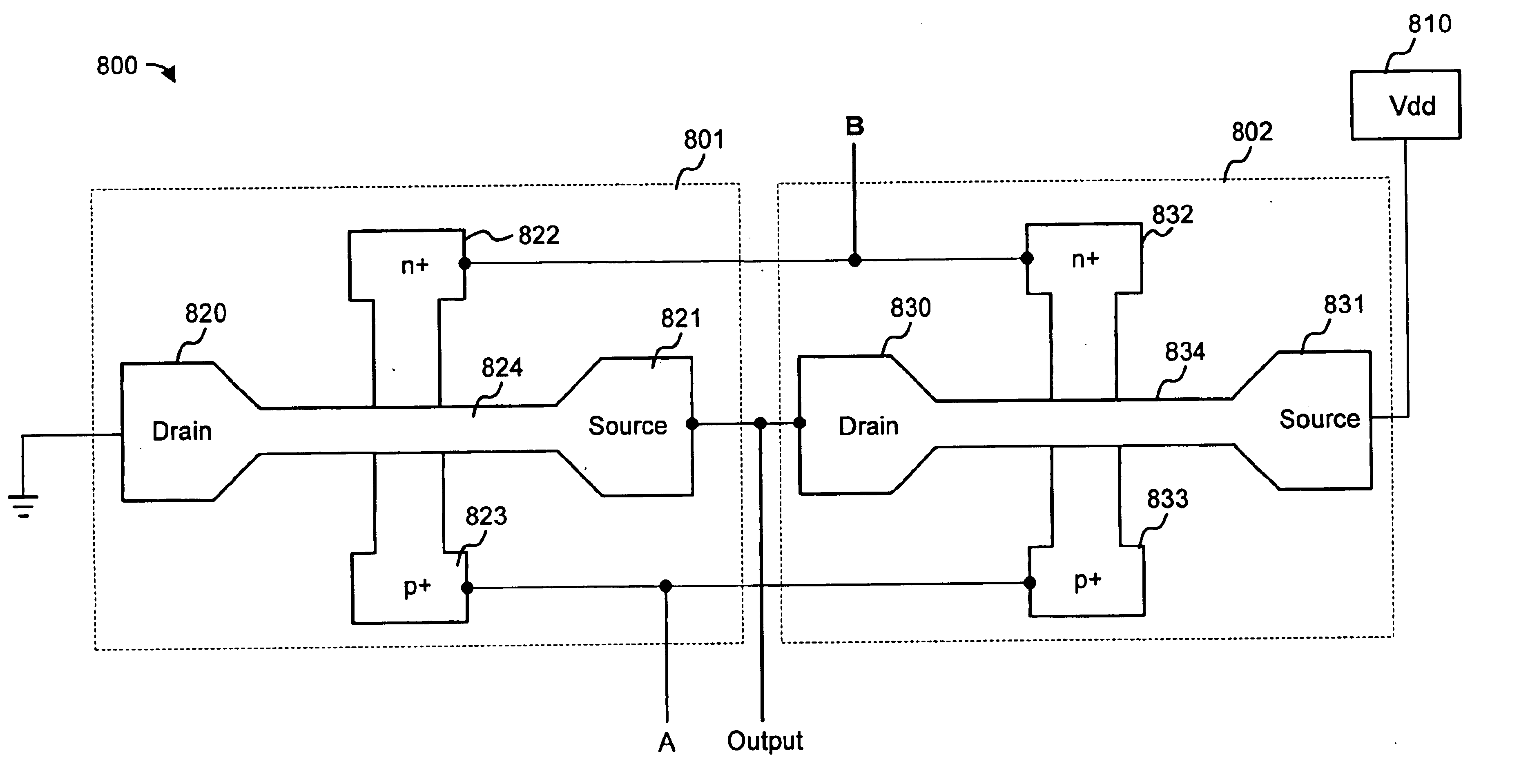
Two transistors are connected together to implement a NOR gate. Each one of the transistors may be an asymmetric FinFET having two separately addressable gates.
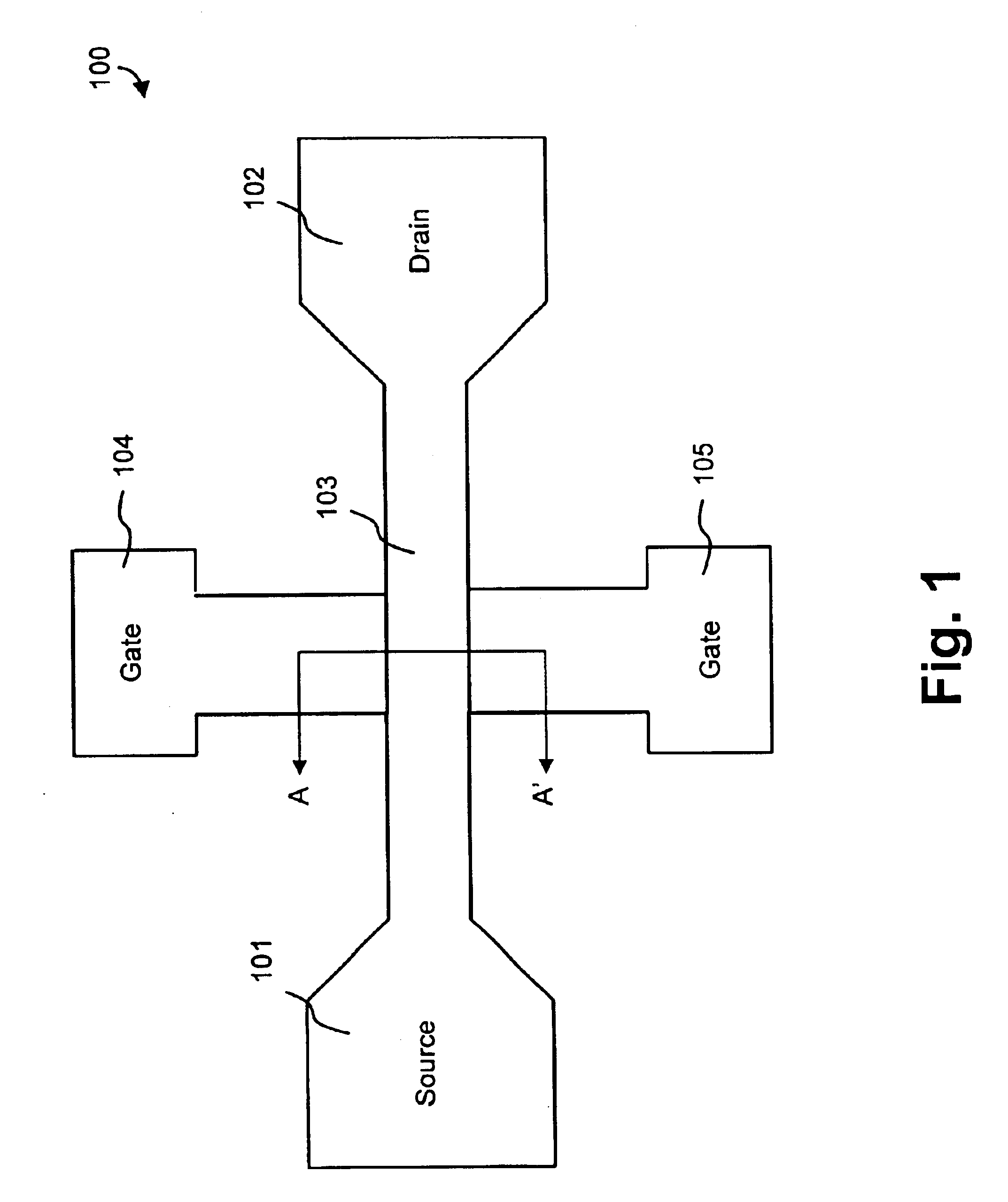
Asymmetric FinFET

A FinFET, as the term is used herein, refers to a type of double-gate MOSFET in which a conducting channel is formed in a vertical Si “fin” controlled by a self-aligned double-gate. FinFETs are known in the art. Although conventional FinFETs are typically described as “double-gate” MOSFETs, the two gates are electrically connected and thus form a single logically addressable gate.

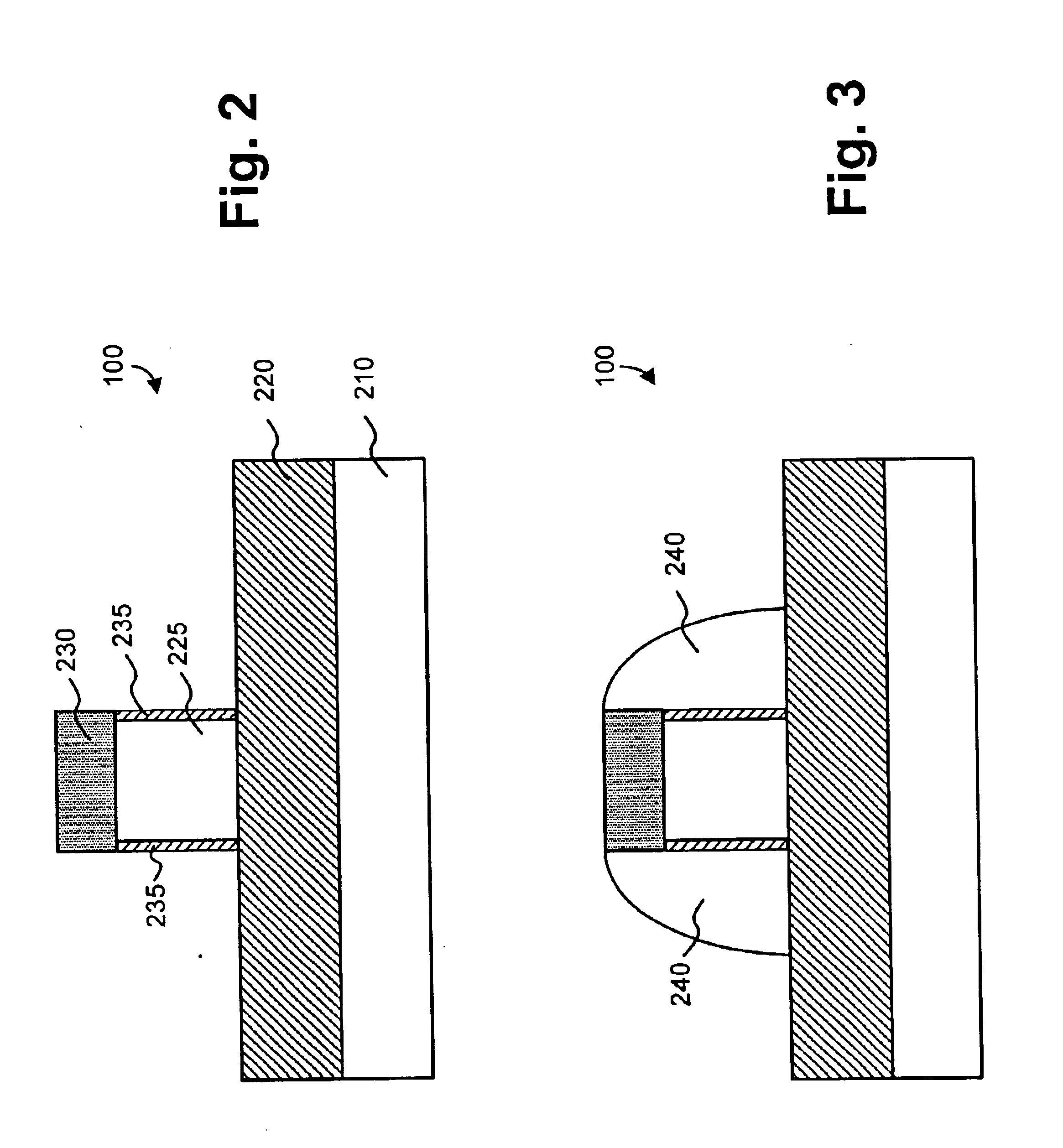
FIG. 1 is a top-level view of a FinFET 100 consistent with principles of the invention. F...


PUM


Abstract

A NOR gate includes is constructed with two asymmetric FinFET type transistors instead of the conventional four-transistor NOR gate. The reduction in the number of transistors from four down to two allows for significant improvements in integrated semiconductor circuits.

Description

BACKGROUND OF THE INVENTIONA. Field of the InventionThe present invention relates generally to semiconductor manufacturing and semiconductor devices and, more particularly, to double gate metal-oxide semiconductor field-effect transistors (MOSFET).B. Description of Related ArtTransistors, such as MOSFETs, are the core building block of the vast majority of semiconductor devices. Some semiconductor devices, such as high performance processors, can include millions of transistors. For these devices, decreasing transistor size, and thus increasing transistor density, has traditionally been a high priority in the semiconductor manufacturing area.Conventional MOSFETs have difficulty scaling below 50 nm fabrication processing. To develop sub-50 nm MOSFETs, double-gate MOSFETs have been proposed. In several respects, the double-gate MOSFETs offer better characteristics than the conventional bulk silicon MOSFETs. These improvements arise because the double-gate MOSFET has a gate electrode o...

Claims


Application Information

Patent Timeline
Patent Type & Authority Patents(United States)
IPC IPC(8): H01L27/085H01L27/088H01L27/092H01L27/12H01L29/423H01L29/786
CPCH01L27/088H01L27/0886H01L27/092H01L29/785H01L27/1203H01L29/42384H01L27/0924H01L29/7856
Inventor KRIVOKAPIC, ZORANAN, JUDY XILINLIN, MING-RENWANG, HAIHONG
Owner GLOBALFOUNDRIES U S INC
Why Eureka
Try Eureka