CMOS circuit based on semi-conductor nano material and preparation therefor

A technology of nanomaterials and semiconductors, applied in the field of nanoelectronics, can solve the problems that the performance of p-type and n-type devices is not very matched, the performance of n-type and p-type field effect transistors is low, and it is not suitable for scale integration, etc., to achieve overall performance Best, improve carrier mobility, reduce scattering effect

Active Publication Date: 2008-03-05
PEKING UNIV
View PDF1 Cites 17 Cited by
  • Summary
  • Abstract
  • Description
  • Claims
  • Application Information

AI Technical Summary

Problems solved by technology

The Avouris group of IBM Corporation used vacuum annealing technology to prepare n-type field effect transistors [V.Derycke, R.Martel, J.Appenzeller, and Ph.Avouris, NanoLetters, 1, 453 (2001)], and obtained a CMOS circuit on this basis , but the performance of both n-type and p-type field effect transistors is low, and n-type devices are unstable
The H.J.Dai research group of Stanford University in the United States used high-current calcination to convert some p-type field effect transistors into n-type, thereby obtaining CMOS circuits [A.Javey, Qian Wang, Ant Ural, Yiming Li, H.Dai, NanoLetters, 2, 929 (2002)], but the performance of the obtained p-type and n-type devices does not match very well, and this method is not suitable for large-scale integration at all

Method used


Image

  • CMOS circuit based on semi-conductor nano material and preparation therefor
  • CMOS circuit based on semi-conductor nano material and preparation therefor
  • CMOS circuit based on semi-conductor nano material and preparation therefor

Examples


Embodiment 1

[0036] Example 1: Single-walled carbon nanotube CMOS inverter with bottom gate structure using Pd and Sc as source and drain electrodes and its preparation

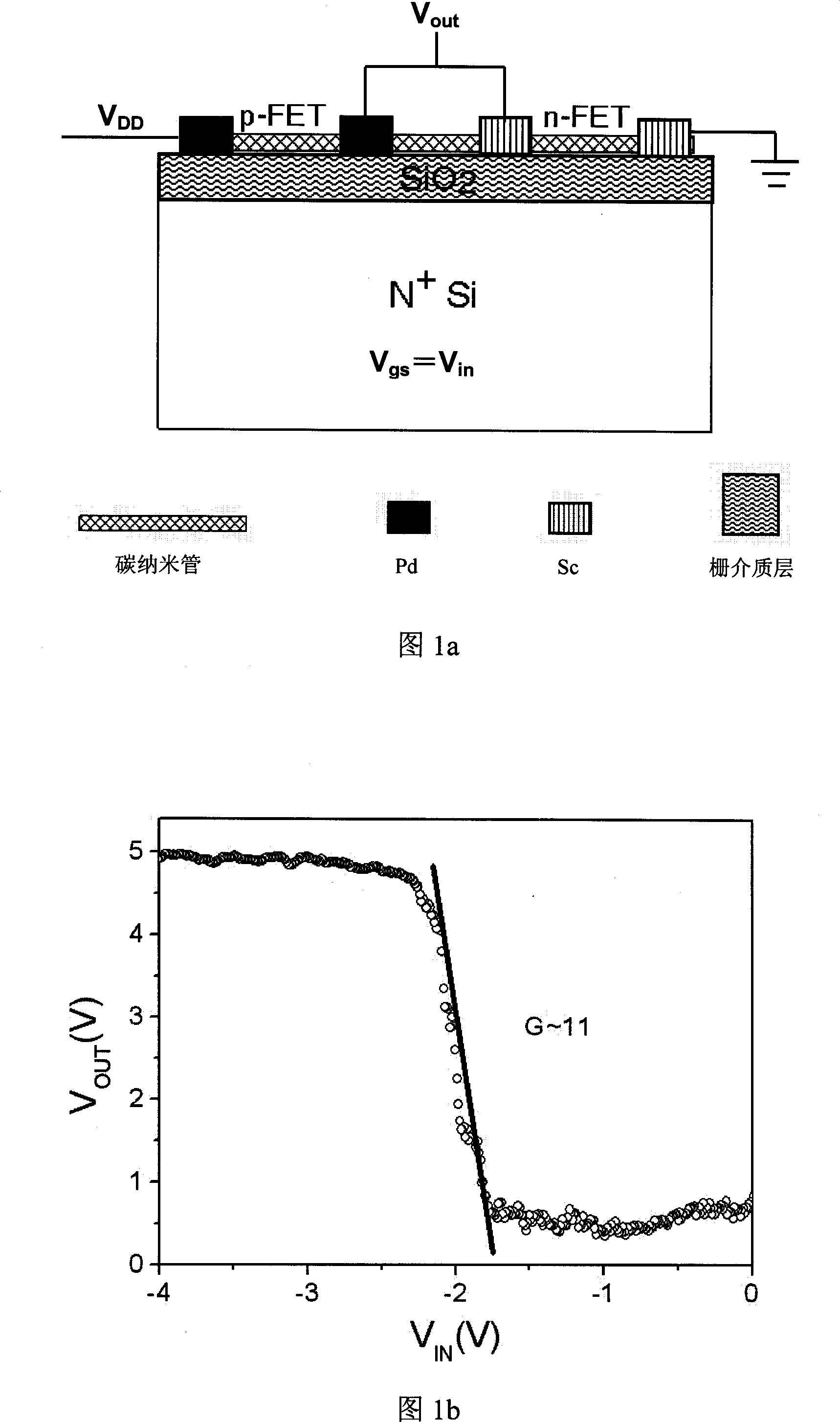
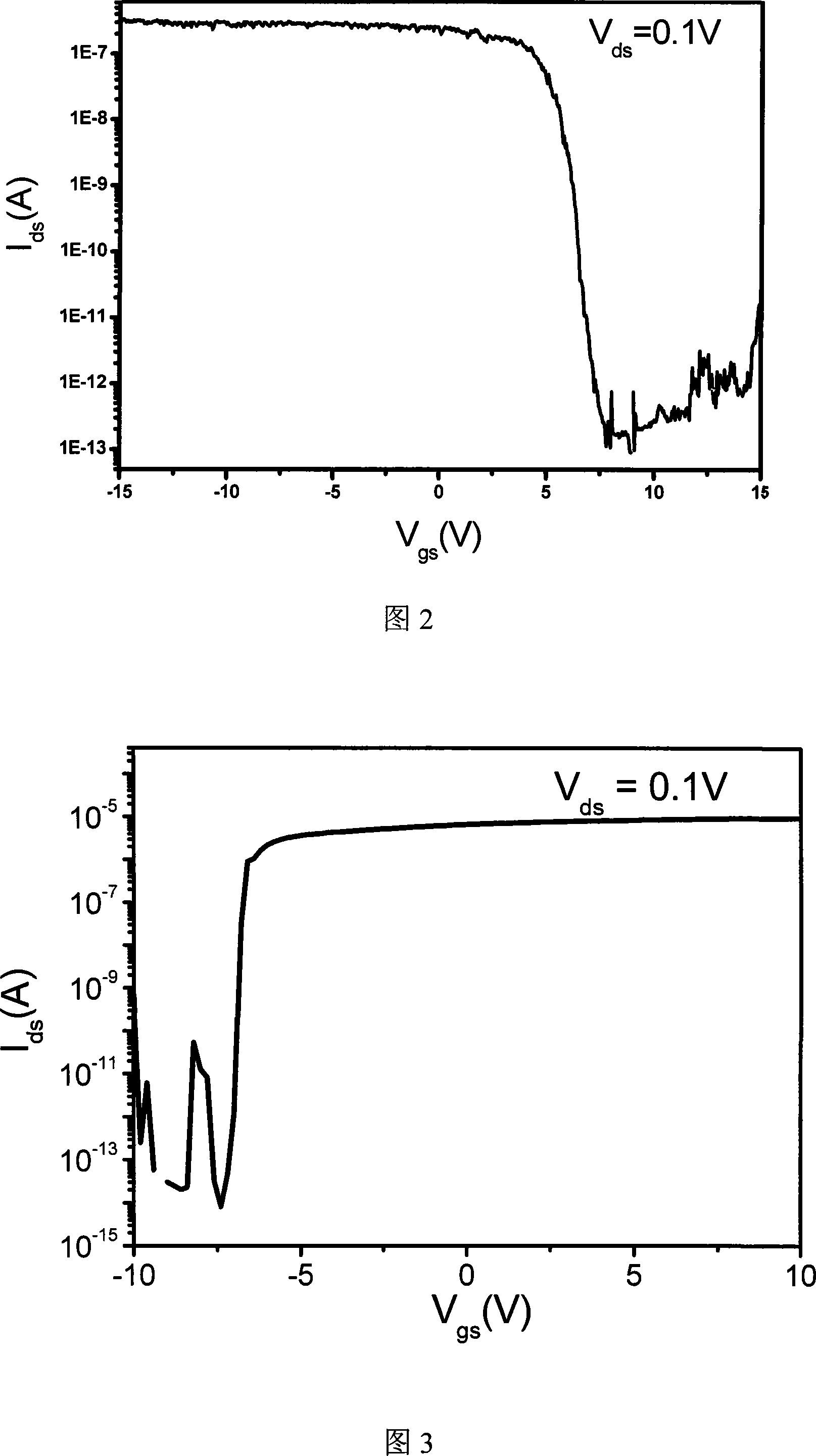
[0037] SiO as shown in Figure 1a 2 Single-walled carbon nanotube CMOS inverter with Si as the gate dielectric and Si as the back gate. On the left, Pd is used as the source (left) and drain (right) electrode material, plus carbon nanotubes between the two electrodes, forming a p-type FET. On the right, Sc is used as the source (right) and drain (left) electrode material, plus carbon nanotubes between the two electrodes, forming an n-type FET. As shown in the figure, connect the drain electrode of the p-type FET to the drain electrode of the n-type FET, and its potential is the output voltage of the inverter. The common bottom gate voltage of the p-type FET and the n-type FET is used as the input voltage Vin, thus forming a CMOS inverter circuit. Concrete preparation steps are as follows:

[0038] 1. By positioning gro...

Embodiment 2

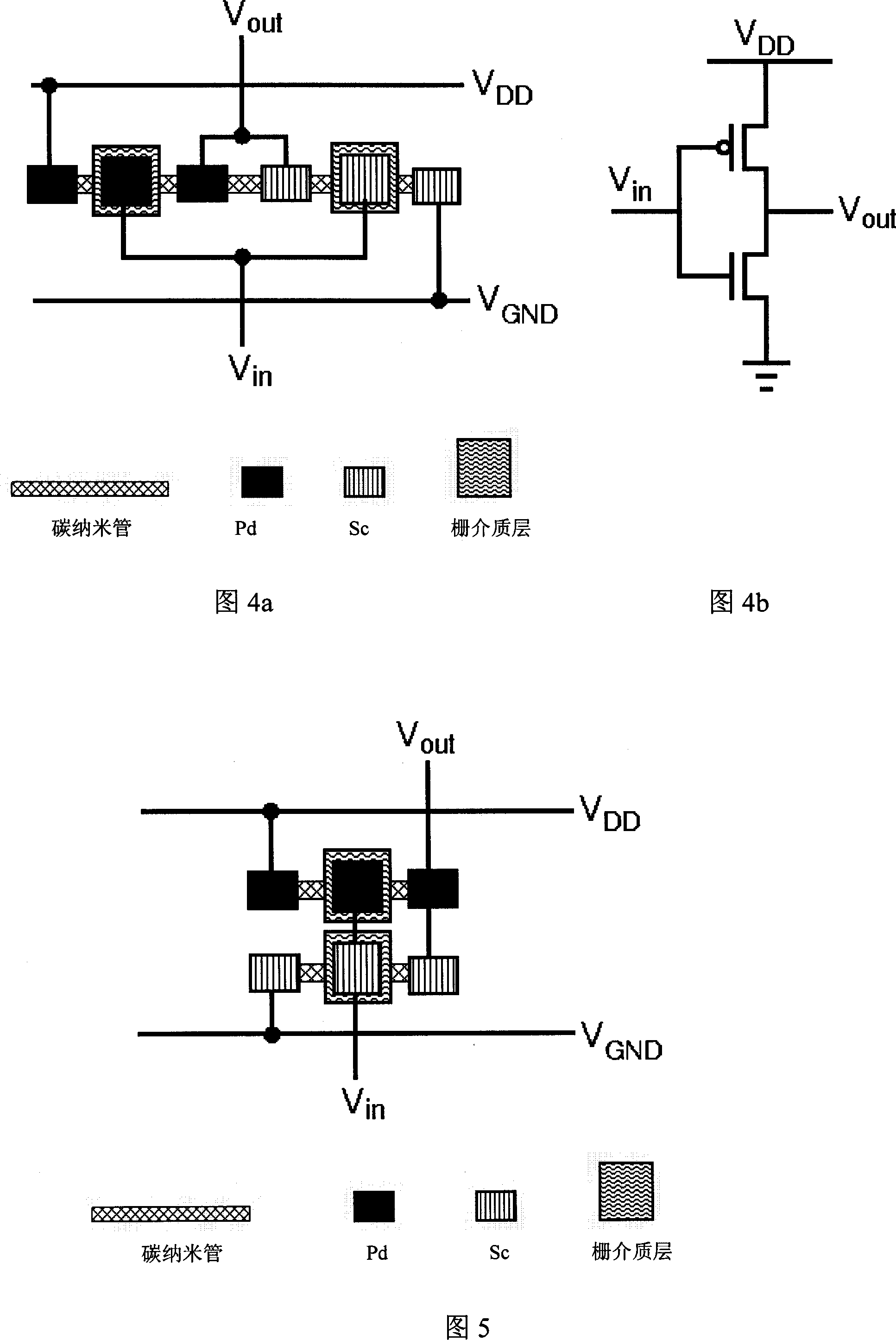
[0046] Example 2: Carbon nanotube CMOS inverter with top gate structure

[0047] As shown in FIG. 4 a and FIG. 5 , a CMOS inverter with a top-gate structure can be fabricated by using steps similar to those in Embodiment 1. Concrete preparation comprises the following steps:

[0048] 1. By positioning growth, or dropping the dispersed carbon tube solution onto the marked substrate to obtain the Si / SiO 2 One or more parallel carbon nanotubes on a substrate;

[0049] 2. Observe and record the specific position of carbon nanotubes through scanning electron microscope or atomic force microscope;

[0050] 3. Apply photoresist on the substrate and form the shape of the gate by optical exposure or electron beam lithography;

[0051] 4. Put the sample into the atomic layer deposition system to grow a gate dielectric layer (ZrO 2 , Al 2 o 3 or HfO 2 ), the growth temperature should not be higher than 170 degrees Celsius;

[0052] 5. Put the sample into acetone to peel off, or u...

Embodiment 3

[0058] Example 3: Carbon nanotube CMOS NAND gate circuit with top gate structure

[0059] As shown in Figure 6a and Figure 7, a carbon nanotube n-type FET and a p-type FET with a top-gate structure can be prepared respectively by steps similar to those in Example 2, and the source, drain electrode and p-type FET are respectively shown in Figure 6a and Figure 7 The gate electrodes are connected as shown in the figure to obtain CMOS NAND gate circuits based on 2 and 1 carbon nanotubes.


PUM


Abstract

This invention puts forward a simple preparing and integrating method for realizing high performance CMOS circuit not doped on one-dimensional semiconductor nm material, in which, the p-type field effect transistor in the CMOS circuit is realized by controlling a metal electrode of high power function to exchange electrons with the valence band of carbon nm tube or other one-dimensional nm materials, the n-type field effect transistor is realized by controlling a metal electrode of low power function to exchange electrons with the conduction band of a carbon nm tube or other one-dimensional semiconductor nm materials directly, besides, this invention applies a back grid and a top grid to realize a basic logic circuit or even more complicated logic circuit of inverters, AND-NOT gates, NOR gates and full-adders.

Description

technical field [0001] The invention belongs to the field of nanoelectronics, in particular to a nano-complementary field-effect transistor (CMOS) circuit based on one-dimensional nano-materials, especially carbon nano-tubes, and its preparation technology. Background technique [0002] The progress of the current microelectronics technology with silicon-based CMOS as the mainstream has benefited to a large extent from the scaling down of devices. The smaller the device, the higher the performance and integration, and the corresponding lower price, these advantages promote the continuous progress of the microelectronics industry. However, as the device scale enters the sub-micron range, the improvement of the performance / price ratio achieved by reducing the device scale alone can no longer balance the resulting difficulties. One of the most serious problems is the uniformity of small-scale devices. Although there have been reports of successful silicon-based field-effect t...

Claims


Application Information

Patent Timeline
Patent Type & Authority Applications(China)
IPC IPC(8): H01L27/092H01L21/8238
Inventor 彭练矛梁学磊陈清张志勇王胜胡又凡姚昆
Owner PEKING UNIV
Why Eureka
Try Eureka