Semiconductor integrated circuit having current leakage reduction scheme

a technology of integrated circuits and threshold voltages, applied in the direction of logic circuits, power consumption reduction, logic circuits characterised by logic functions, etc., can solve the problems of long propagation delay, drawbacks of conventional dual threshold schemes, and increased power consumption of semiconductor ics based on such lowered threshold voltages. achieve the effect of low power consumption

Inactive Publication Date: 2007-11-06
CONVERSANT INTPROP MANAGEMENT INC
View PDF6 Cites 17 Cited by
  • Summary
  • Abstract
  • Description
  • Claims
  • Application Information

AI Technical Summary

Benefits of technology

[0013]It is an object of the present invention to provide an improved semiconductor IC capable of operating with low power consumption.
[0017]For example, the feedback signal is a combination of output of the CMOS inverter and an additional input logic signal that has an earlier transition than the input logic signal. With the feedback signal, a self leakage reduction function is performed for an off transistor of the NMOS and PMOS transistors of the CMOS inverter. Thus, the leakage path current is suppressed and there is no need to have special “power saving” signals. It can reduce leakage current in active operation mode as well as standby mode. Therefore, the semiconductor IC is capable of operating at high speed and with low power consumption even when the semiconductor IC is not in the specific power down mode.
[0023]The present invention generally relates to semiconductor ICs and in particular to low power ICs. The present invention uses a feedback scheme to reduce the leakage current, so there is no need to have special “power saving” signals, and can reduce leakage current in active operation mode as well as standby mode.

Problems solved by technology

However, the lowered threshold voltage results in significant sub-threshold leakage (i.e., leakage current present for transistor gate voltages below a threshold voltage) and therefore, semiconductor ICs based on such lowered threshold voltages consume more power in normal operation as well as power-down mode operation.
However, such conventional dual threshold scheme has a drawback.
When the input logic signal IN transitions from “low” logic state to “high” logic state, it causes a longer propagation delay.
In the normal operation mode, there are still current leakage paths, resulting in current leakages and great total active power consumption.

Method used


Image

  • Semiconductor integrated circuit having current leakage reduction scheme
  • Semiconductor integrated circuit having current leakage reduction scheme
  • Semiconductor integrated circuit having current leakage reduction scheme

Examples


Embodiment Construction

[0045]In the following detailed description of sample embodiments of the invention, reference is made to the accompanying drawings which form a part hereof, and in which is shown by way of illustration specific sample embodiments in which the present invention may be practiced. These embodiments are described in sufficient detail to enable those skilled in the art to practice the present invention, and it is to be understood that other embodiments may be utilized and that logical, mechanical, electrical, and other changes may be made without departing from the scope of the present invention. The following detailed description is, therefore, not to be taken in a limiting sense, and the scope of the present invention is defined by the appended claims.

[0046]Generally, the present invention provides semiconductor integrated circuits with low power consumption. The present invention is applicable to any type of logic gates.

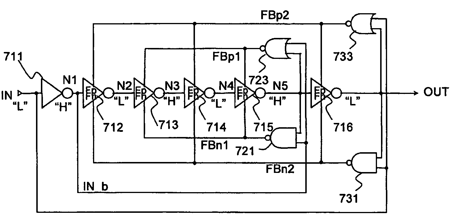
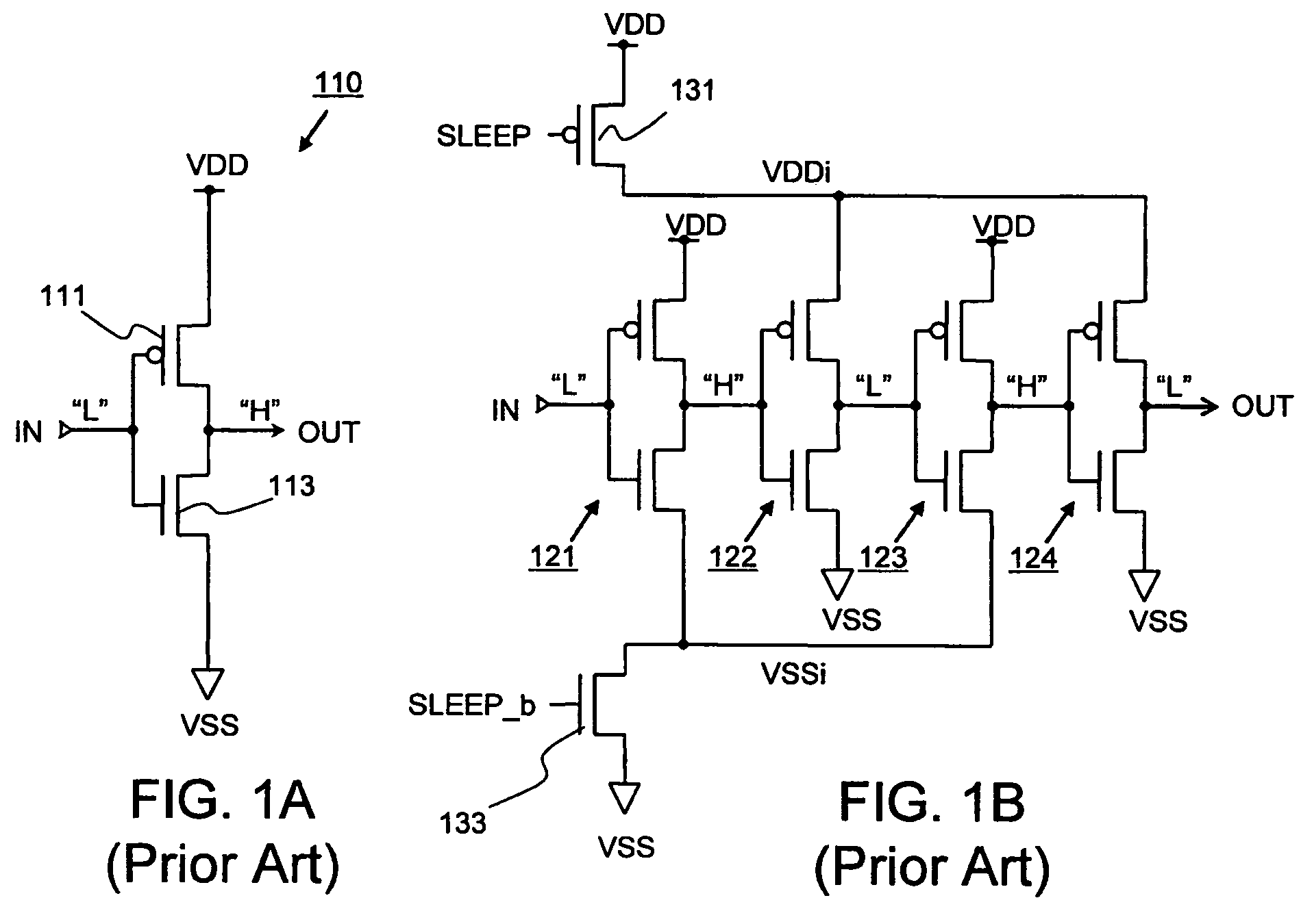
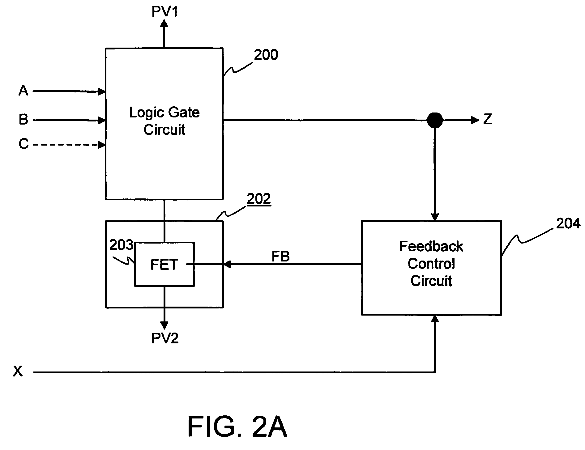
[0047]FIG. 2A illustrates one aspect of the present invention. Re...


PUM


Abstract

A semiconductor integrated circuit includes a CMOS controlled inverter consisting of series-connected PMOS and NMOS transistors. The source of the NMOS transistor is coupled to a ground line through an additional NMOS transistor for power gating of voltage VSS. The source of the PMOS transistor can be coupled to a power supply line through an additional PMOS transistor for power gating of voltage VDD. The inverter receives an input signal IN and its complementary version that has transitioned earlier than the input signal. In response to the input signal, the inverter produces an output signal. A NAND gate that receives the output signal and the complementary input signal controls the power gating NMOS transistor. A NOR gate that receives the output signal and the complementary input signal controls the power gating PMOS transistor. The power gating to the CMOS inverter is performed by feedback of the output signal and the complementary input signal, with the result that current leakage reduction through the CMOS controlled inverter is achieved. A self leakage reduction with power gating transistors is applicable to another type of logic gates such as NAND, NOR and Exclusive-OR, AND, OR.

Description

TECHNICAL FIELD[0001]The present invention generally relates to semiconductor integrated circuits and in particular to semiconductor integrated circuits with low power consumption requirements.BACKGROUND INFORMATION[0002]In order to obtain a high-speed operation and high-density integrated circuits (ICs) for the purpose of cost reduction, deep sub-micron CMOS processes like 90 nm, 65 nm, 45 nm have been introduced and implemented in many semiconductor IC devices. For those deep sub-micron processes, MOS transistors have to be scaled down (i.e., have minimum transistor dimensions decreased) and threshold voltage Vth of the transistors have to be lowered. However, the lowered threshold voltage results in significant sub-threshold leakage (i.e., leakage current present for transistor gate voltages below a threshold voltage) and therefore, semiconductor ICs based on such lowered threshold voltages consume more power in normal operation as well as power-down mode operation.[0003]In the d...

Claims


Application Information

Patent Timeline
Patent Type & Authority Patents(United States)
IPC IPC(8): H03K17/16H03K19/003
CPCH03K19/0016H01L27/092H01L2924/0002H01L2924/00H01L23/58H01L27/00H03K17/14H03K19/0948
Inventor OH, HAKJUNE
Owner CONVERSANT INTPROP MANAGEMENT INC
Why Eureka
Try Eureka