Built-in self test circuit for analog-to-digital converter and phase lock loop and the testing methods thereof

a self-testing, analog-to-digital converter technology, applied in the field of circuits, can solve problems such as the inability to accurately test the method described in fig. 2 and achieve the effect of improving the measuring precision

Inactive Publication Date: 2008-05-29
FARADAY TECH CORP
View PDF5 Cites 17 Cited by
  • Summary
  • Abstract
  • Description
  • Claims
  • Application Information

AI Technical Summary

Benefits of technology

[0009]The invention provides a BIST circuit for testing an ADC and a PLL, comprising a controllable delay circuit, a calculating logic and a charge-discharge circuit. The controllable delay circuit has a first input terminal for receiving a test signal and adjusting a delay of the test signal according to a first control signal and outputting a delay signal at a first output terminal. The calculating logic calculates a difference between a signal under test and the delay signal to generate a clock width which is further used to control the charge-discharge circu...

Problems solved by technology

Due to large clock width, the precision of...

Method used


Image

  • Built-in self test circuit for analog-to-digital converter and phase lock loop and the testing methods thereof
  • Built-in self test circuit for analog-to-digital converter and phase lock loop and the testing methods thereof
  • Built-in self test circuit for analog-to-digital converter and phase lock loop and the testing methods thereof

Examples


Embodiment Construction

[0022]The following description is of the best-contemplated mode of carrying out the invention. This description is made for the purpose of illustrating the general principles of the invention and should not be taken in a limiting sense. The scope of the invention is best determined by reference to the appended claims.

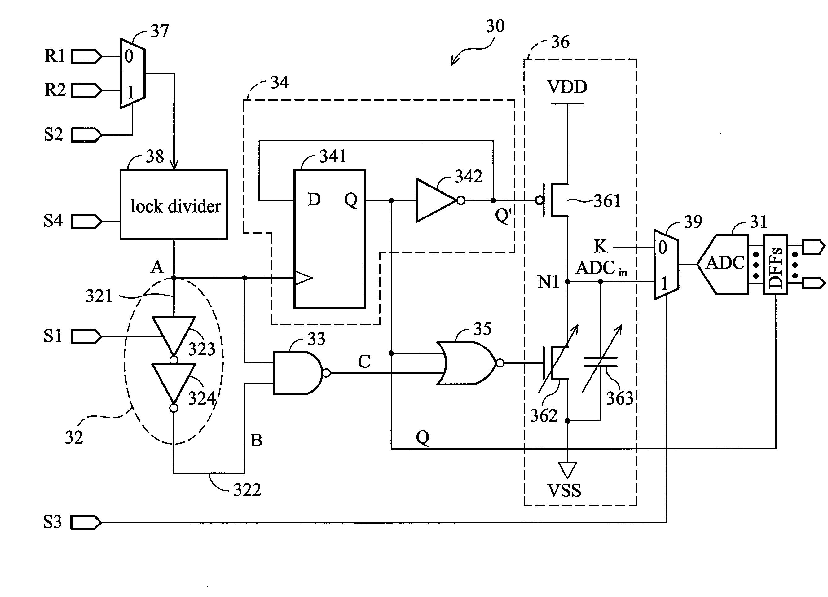
[0023]FIG. 3A shows a BIST circuit 30, according to an embodiment of the invention, for testing performance of ADC 31 and period jitters of the phase lock loop. BIST circuit 30 comprises controllable delay circuit 32, NAND gate 33, dividing circuit 34, NOR gate 35 and charge-discharge circuit 36. [0021] Controllable delay circuit 32 has a first input terminal for receiving a test signal A. The delay from test signal A to delay signal B is adjusted by controllable delay circuit 32 according to a first control signal SI which may be the digital bus, and delay signal B is output from a first output terminal 322. Test signal A and delay signal B are received by NAND gate 3...


PUM


Abstract

A BIST circuit for testing both an analog-to-digital converter and a phase lock loop includes a controllable delay circuit, a NAND gate, a dividing circuit, a NOR gate and a charge/discharge circuit. The invention reduces the period of the signal under test, converts its pulse width to voltage and measures the output via an ADC. The clock jitter becomes sensitive through a delay cancellation method, thus, the accuracy is improved. The invention further comprises all testing procedure for period jitters of a PLL and static characteristics of an ADC. The test error caused by process variation can be corrected by a controllable delay circuit such that the error determination of the test result is prevented.

Description

BACKGROUND OF THE INVENTION[0001]1. Field of the Invention[0002]The invention relates to a circuit, and more particularly to a built-in self test (BIST) circuit for testing not only the differential non-linearity(DNL) error and the integral non-linearity(INL) error of an analog-to-digital converter(ADC) but also the period jitters of a clock signal. The clock signal can be outputs of an oscillator or a phase lock loop.[0003]2. Description of the Related Art[0004]A phase lock loop (PLL) is widely used in frequency synthesization, clock correction, clock distribution and phase demodulation. Frequency synthesization, clock correction, clock distribution and phase demodulation are generally used in optical fiber links, radio phones and computers. Clock variations such as period jitters of the phase lock loop circuit may degrade performance and limit applications of the phase lock loop circuit. Thus, for high-speed applications, precise and cost effective measurement on clock variation a...

Claims


Application Information

Patent Timeline
IPC IPC(8): G06F19/00G06F11/25G06F11/27G01R29/26
CPCG06F11/24G01R31/3167
Inventor CHANG, YEONG-JAR
Owner FARADAY TECH CORP
Why Eureka
Try Eureka