Internal voltage generating circuit for periphery, semiconductor memory device having the circuit and method thereof

a technology of internal voltage generation and circuit, which is applied in the field of internal voltage generation circuit, can solve the problems of insufficient power supply and power supply, and achieve the effect of effectively controlling the internal voltage and preventing unnecessary power consumption

Inactive Publication Date: 2005-01-11
SAMSUNG ELECTRONICS CO LTD
View PDF5 Cites 23 Cited by
  • Summary
  • Abstract
  • Description
  • Claims
  • Application Information

AI Technical Summary

Benefits of technology

Thus according to the disclosed embodiments, the internal voltage can be supplied only to peripheral circuits of selected banks, as needed, thereby preventing unnecessary power consumption, effectively controlling the internal voltage, and always properly supplying the internal voltage.

Problems solved by technology

It is recognized herein that problems can arise with such implementations, problems such as power being supplied when the peripheral circuits are not needed, or insufficient power being supplied at other times.

Method used


Image

  • Internal voltage generating circuit for periphery, semiconductor memory device having the circuit and method thereof
  • Internal voltage generating circuit for periphery, semiconductor memory device having the circuit and method thereof
  • Internal voltage generating circuit for periphery, semiconductor memory device having the circuit and method thereof

Examples


first embodiment

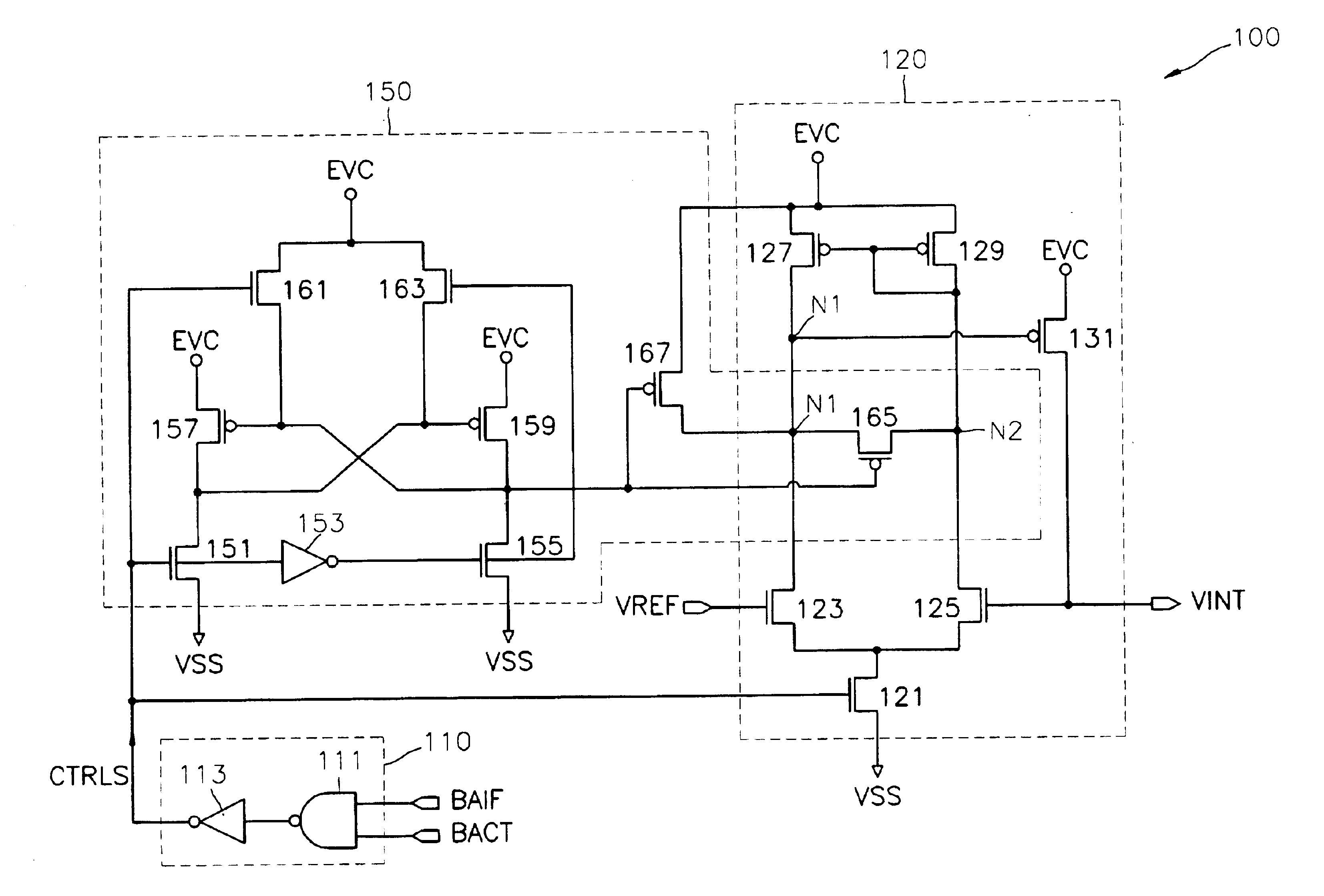
Referring to FIG. 1, a switchable internal voltage generator 100 according to the present invention includes a control section 110 to generate a control signal CTRLS in response to a bank activation command BACT and a bank activation signal BAIF (which enables memory access to a given memory bank), and an internal voltage generating circuit 120 to respond to the control signal CTRLS. Circuit 120 receives a reference voltage VREF, and when switched on maintains an internal voltage VINT equal to the reference voltage VREF.

The control signal CTRLS is enabled when the bank activation command BACT and the bank activation signal BAIF are concurrently enabled.

The operation of the switchable internal voltage generating circuit 100 will now be described with reference to FIG. 1.

The bank activation command BACT is an external command for enabling banks in a semiconductor memory device. When banks are selected by a bank address after the bank activation command BACT is applied, the selected ba...

second embodiment

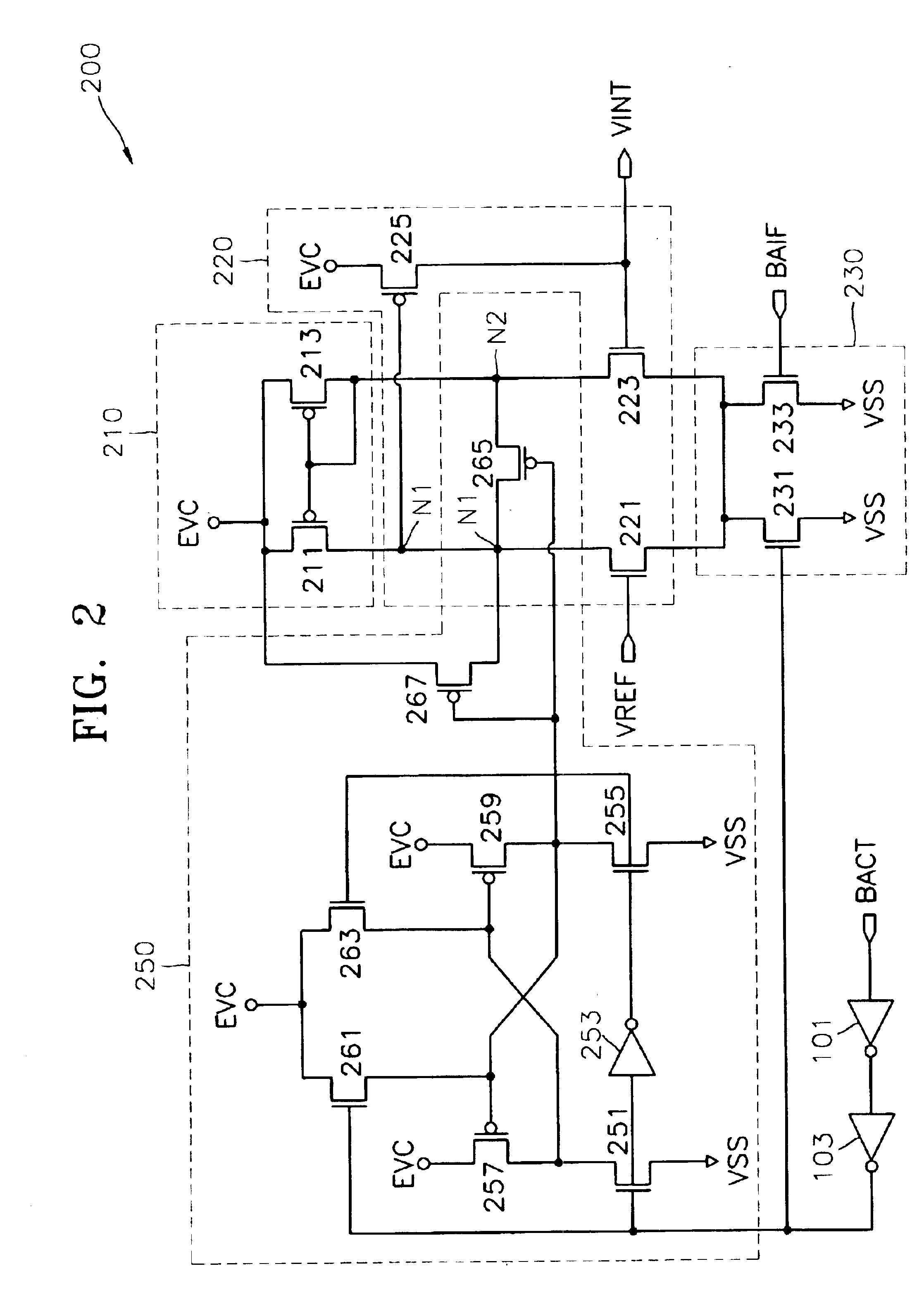
Referring to FIG. 2, a switchable internal voltage generator 200 according to the present invention includes a current mirror 210, a differential amplifier and input section 220, and a current sink 230.

The current mirror 210 is connected to an external voltage (EVC) and includes first and second MOS transistors 211 and 213, forming a current mirror.

The differential amplifier and input section 220 includes a third MOS transistor 221, having a gate connected to a reference voltage (VREF), a fourth MOS transistor 223, having a gate connected to an internal voltage (VINT) to be controlled equal to the reference voltage (VREF), and a fifth MOS transistor 225 that is connected between the EVC and the gate of the fourth MOS transistor 223 and has its gate connected to one end of the first MOS transistor 211.

The current sink 230 is controlled by a bank activation command BACT and a bank activation signal BAIF, and controls VINT in response to the bank activation signal BAIF.

More specificall...


PUM


Abstract

An internal voltage generator for memory bank peripheral circuitry, a semiconductor memory device having the internal voltage generator, and a method for generating an internal voltage are provided. A switchable internal voltage generating circuit according to the present invention includes a control section and an internal voltage generating circuit. The control section generates a control signal in response to a bank activation command and a bank activation signal for enabling memory banks. The internal voltage generating circuit receives a reference voltage, and responds to the control signal to output an internal voltage equal to the reference voltage. The control signal is enabled when the bank activation command and the bank activation signal are concurrently enabled. The bank activation signal is generated in response to a bank address. The internal voltage can be supplied only to peripheral circuits of the banks selected by the bank address, thereby preventing unnecessary power consumption, effectively controlling the internal voltage, and always properly supplying the internal voltage.

Description

BACKGROUND OF THE INVENTION1. Field of the InventionThe present invention relates to a semiconductor memory device, and more particularly, to an internal voltage generating circuit for receiving an external voltage having a predetermined level and converting the external voltage into an internal voltage to supply power to peripheral circuits of banks, a semiconductor memory device having the internal voltage generating circuit, and a method for generating an internal voltage.2. Description of the Related ArtRecently, an internal voltage generating circuit for maintaining an internal power voltage at a predetermined level independent of an external power voltage has been used in semiconductor memory devices operating in the region of 3V to 6V to improve properties such as high-speed operation and low operating current. With the increased operating current drawn by semiconductor products that are designed to operate at a low supply voltage of 3.3V using an external voltage (EVC), semi...

Claims


Application Information

Patent Timeline
Patent Type & Authority Patents(United States)
IPC IPC(8): G11C5/14G11C11/413
CPCG11C11/413G11C5/14G11C5/147G11C11/4074
Inventor KIM, JAE-HOONYOUN, JAE-YOUN
Owner SAMSUNG ELECTRONICS CO LTD
Why Eureka
Try Eureka