Activation of word lines in semiconductor memory device

a technology of word line and memory device, which is applied in the direction of information storage, static storage, digital storage, etc., can solve the problems of wasting power, more expensive, and having a lower capacity than dram, and achieve the effect of reducing the power consumption associated with word line activation

Inactive Publication Date: 2005-01-11
SEIKO EPSON CORP
View PDF30 Cites 10 Cited by
  • Summary
  • Abstract
  • Description
  • Claims
  • Application Information

AI Technical Summary

Benefits of technology

An object of the present invention is to provide a technique for reducing the p...

Problems solved by technology

SRAM, on the other hand, while easier to use due to the lack of a need for refresh operations, is more expensive and has lower capacity than DRAM.
However, in instances where, for example, the same word line is activated during consecutive cycles, repeated...

Method used


Image

  • Activation of word lines in semiconductor memory device
  • Activation of word lines in semiconductor memory device
  • Activation of word lines in semiconductor memory device

Examples


Embodiment Construction

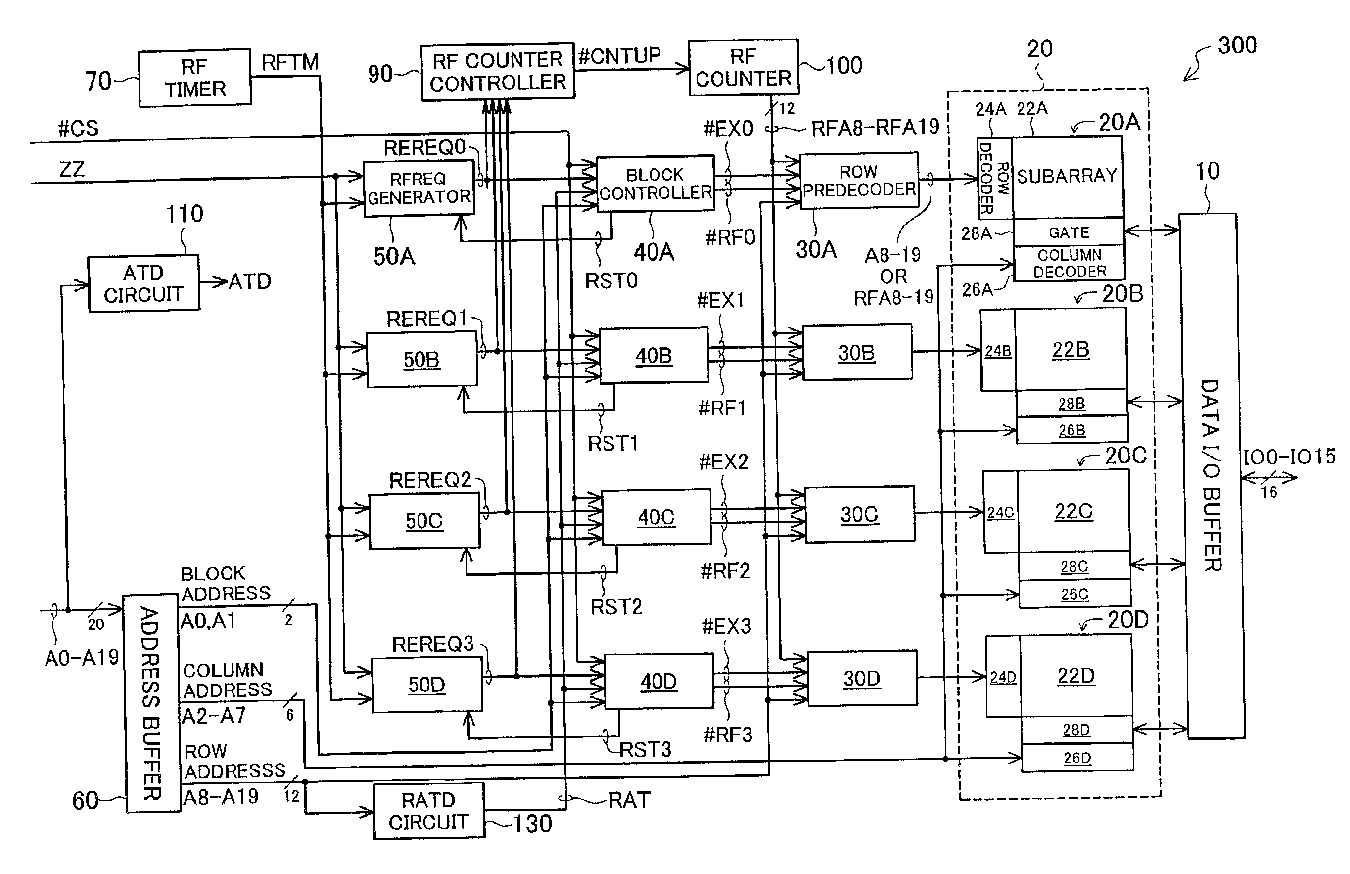
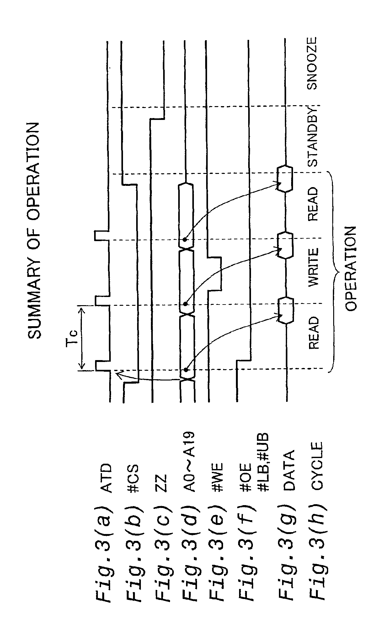
An exemplary embodiment of the invention is described in the following order.A. Summary of memory chip pinout and operating modes:B. Overall memory chip internal design:C. Internal design of word line activation controller:D. Operation of word line activation controller:D1. Operation during operation cycle (with no refresh request):D2. Operation during operation cycle (with a refresh request):D3. Operation in standby cycle and snooze mode:E. Example of application in an electronic device:

A. Summary of Memory Chip Pinout and Operating Modes:

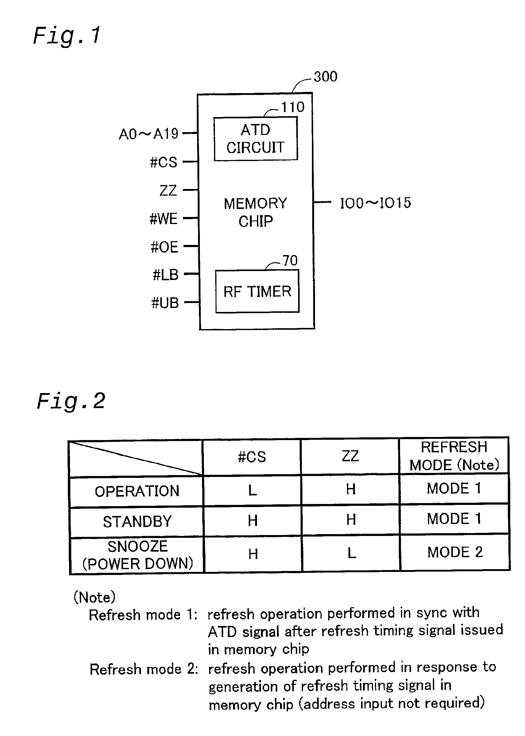
FIG. 1 is an illustrative diagram showing the pinout of a memory chip 300 pertaining an embodiment of the invention. Memory chip 300 has the following terminals.A0-A19: address input terminals (20)#CS: chip select input terminalZZ: snooze input terminal#WE: write enable input terminal#OE: output enable input terminal#LB: lower byte enable input terminal#UB: upper byte enable input terminalIO0-IO15: I / O data terminals (16)

In the following discussio...


PUM


Abstract

To provide a technique for reducing the power consumption associated with word line activation in a semiconductor memory device. The semiconductor memory device is provided with a word line activation controller for controlling word line activation. Where consecutive operation cycles use multiple-bit addresses that include an identical row address, the word line activation controller can maintain an the activated state of a word line activated during an initial cycle of the consecutive cycles, without deactivating it until a final cycle of the consecutive cycles. If a refresh operation is to be performed during a cycle among the consecutive cycles after the initial cycle, the word line activation controller can deactivate the activated word line prior to performing the refresh operation.

Description

BACKGROUND OF THE INVENTION1. Field of the InventionThe present invention relates to control of word line activation in a semiconductor memory device.2. Description of the Related ArtCommonly used semiconductor memory devices include DRAM and SRAM. It is common knowledge that while DRAM offers higher capacity at lower price than SRAM, it requires refresh operations. SRAM, on the other hand, while easier to use due to the lack of a need for refresh operations, is more expensive and has lower capacity than DRAM.Virtual SRAM (known as VSRAM or PSRAM) is a semiconductor memory device that offers that advantages of both DRAM and SRAM. Virtual SRAM has a memory cell array composed of dynamic memory cells identical to those in DRAM, and also houses a refresh controller that allows refresh operations to be performed internally. Thus, external devices connected to virtual SRAM (such as a CPU) can access (i.e., read or write data) virtual SRAM without being aware of refresh operations. This f...

Claims


Application Information

Patent Timeline
IPC IPC(8): G11C8/00G11C8/08G11C11/407G11C11/401G11C11/403G11C11/406
CPCG11C8/08
Inventor MIZUGAKI, KOICHIOTSUKA, EITARO
Owner SEIKO EPSON CORP
Why Eureka
Try Eureka