Semiconductor device
a technology of semiconductors and devices, applied in semiconductor/solid-state device details, multi-purpose tools, diodes, etc., can solve problems such as dielectric breakdown in insulating materials, and achieve the effect of reducing the occurrence of dielectric breakdown
- Summary
- Abstract
- Description
- Claims
- Application Information
AI Technical Summary
Benefits of technology
Problems solved by technology
Method used
Image
Examples
first preferred embodiment
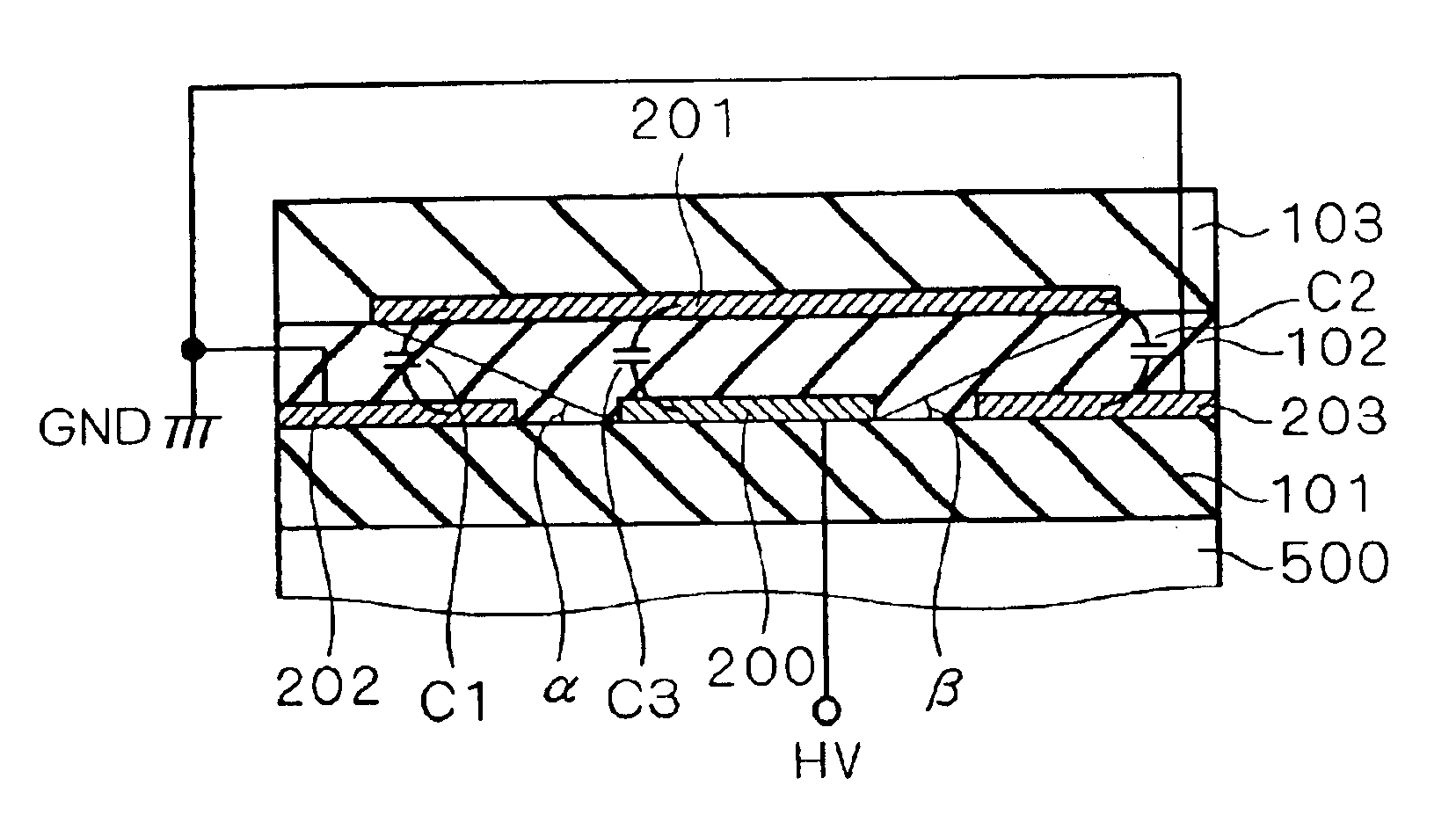
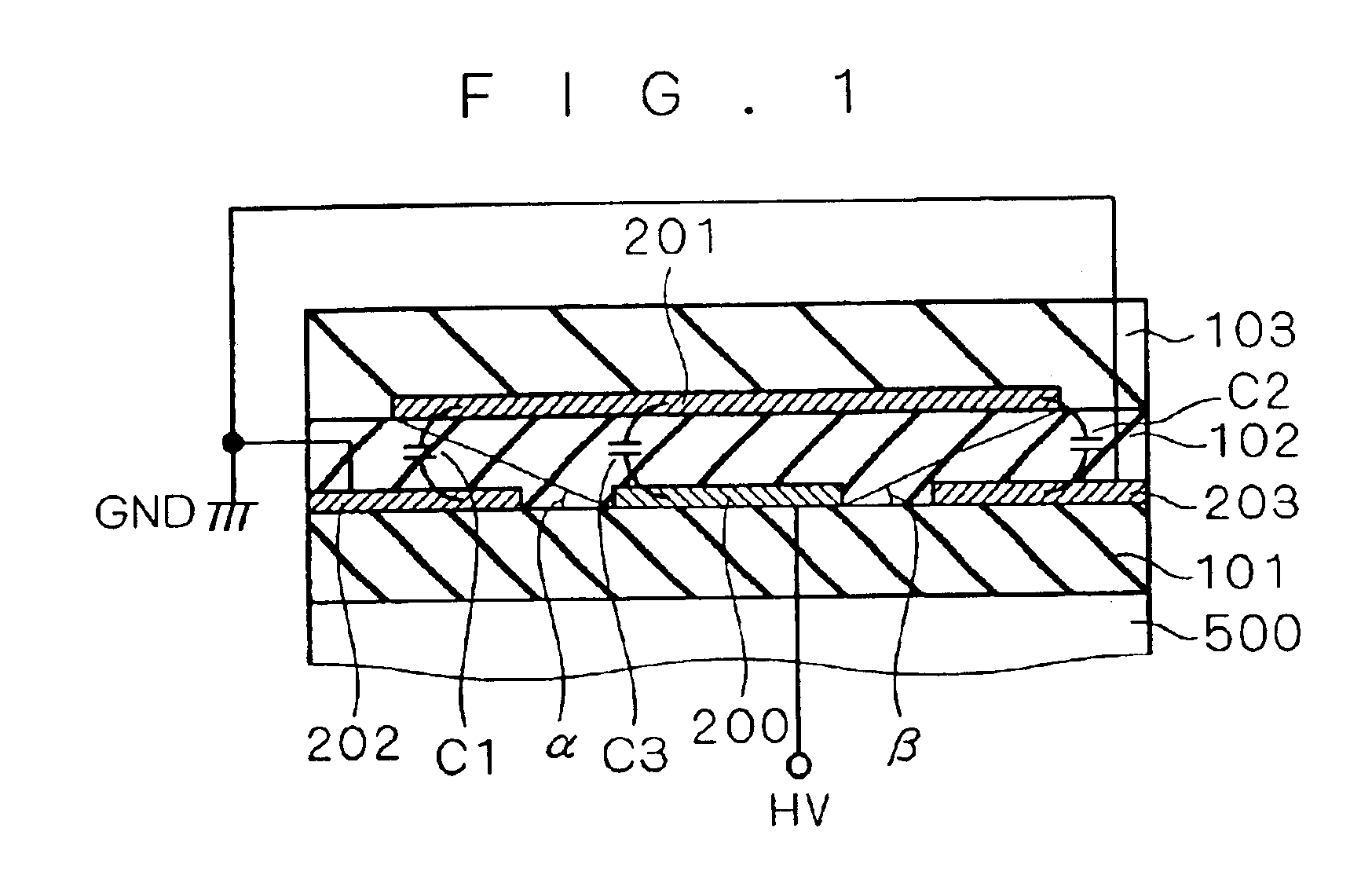
FIG. 1 is a cross-sectional view of a semiconductor device according to a first preferred embodiment of the present invention. Insulating layers 101, 102 and 103 are deposited on a semiconductor substrate 500 in this order. In the following description, a direction toward the insulating layers 101, 102 and 103 as viewed from the semiconductor substrate 500 is referred to as an upward direction and a direction opposite to that direction as a downward direction. For example, the insulating layer 103 lies “above” the semiconductor substrate 500, or the semiconductor substrate 500 lies “under” the insulating layer 103. Electrodes 200, 202 and 203 are formed in a same layer in the vicinity of the boundary between the insulating layers 101 and 102, and an electrode 201 is formed in the vicinity of the boundary between the insulating layers 102 and 103. Such a structure can be obtained by, for example, successively forming the insulating layer 101, the electrodes 200, 202 and 203, the insu...
second preferred embodiment
FIG. 5 is a cross-sectional view of a semiconductor device according to a second preferred embodiment of the present invention. The insulating layers 101, 102 and 103 are deposited on the substrate 500 in this order. The electrode 200 applied with the high potential HV is formed in the vicinity of the boundary between the insulating layers 101 and 102, and the floating electrode 201 and the electrodes 202 and 203 applied with the low potential GND are formed in a same layer in the vicinity of the boundary between the insulating layers 102 and 103. Such a structure can be obtained by, for example, successively forming the insulating layer 101, the electrode 200, the insulating layer 102, the floating electrode 201 and the electrodes 202 and 203, and the insulating layer 103 on the semiconductor substrate 500.
The electrode 200 extends along a direction perpendicular to the plane of the drawing and the floating electrode 201 covers above the electrode 200 in the high-potential intercon...
third preferred embodiment
FIG. 7 is a cross-sectional view of a semiconductor device according to a third preferred embodiment of the present invention. The insulating layers 101, 102 and 103 are deposited on the substrate 500 in this order. The electrode 200 applied with the high potential HV, floating electrodes 202b and 203, and an electrode 202a applied with the low potential GND are formed in the vicinity of the boundary between the insulating layers 101 and 102, and the floating electrode 201 is formed in the vicinity of the boundary between the insulating layers 102 and 103. The electrodes 202b and 203 are connected to each other and located in the same layer as the electrode 200. Such a structure can be obtained by, for example, successively forming the insulating layer 101, the electrodes 200 and 202a and the floating electrodes 202b and 203, the insulating layer 102, the floating electrode 201, and the insulating layer 103 on the semiconductor substrate 500.
The electrode 200 extends along a directi...
PUM
 Abstract
Description
Claims
Application Information


