Organic electroluminescent device compensated pixel driver circuit

a technology of electroluminescent devices and driver circuits, applied in the direction of instruments, static indicating devices, etc., can solve the problems of limiting the device channel length of polysilicon tfts, affecting image quality, and limiting the design of transistors tsub>2 /sub>, and other problems

Inactive Publication Date: 2005-01-25
SEIKO EPSON CORP
View PDF9 Cites 24 Cited by
  • Summary
  • Abstract
  • Description
  • Claims
  • Application Information

AI Technical Summary

Benefits of technology

According to a third aspect of the present invention there is provided an organic electroluminescent display device comprising one or more compensated pixel driver circuits according to the first aspect of the invention.

Problems solved by technology

There are problems associated with TFT analog circuits and OELDs do not act like perfect diodes.
The effect of such variation in an OELD display, exacerbated by the non perfect diode behaviour, is the non-uniform pixel brightness over the display panel, which seriously affects the image quality.
This issue limits the device channel length of the polysilicon TFTs because of the increase of the short channel effect in polysilicon TFTs when the device channel length gets smaller.
This limitation on the design of transistor T2 is a very serious practical problem, especially when small data currents are used.

Method used


Image

  • Organic electroluminescent device compensated pixel driver circuit
  • Organic electroluminescent device compensated pixel driver circuit
  • Organic electroluminescent device compensated pixel driver circuit

Examples


Embodiment Construction

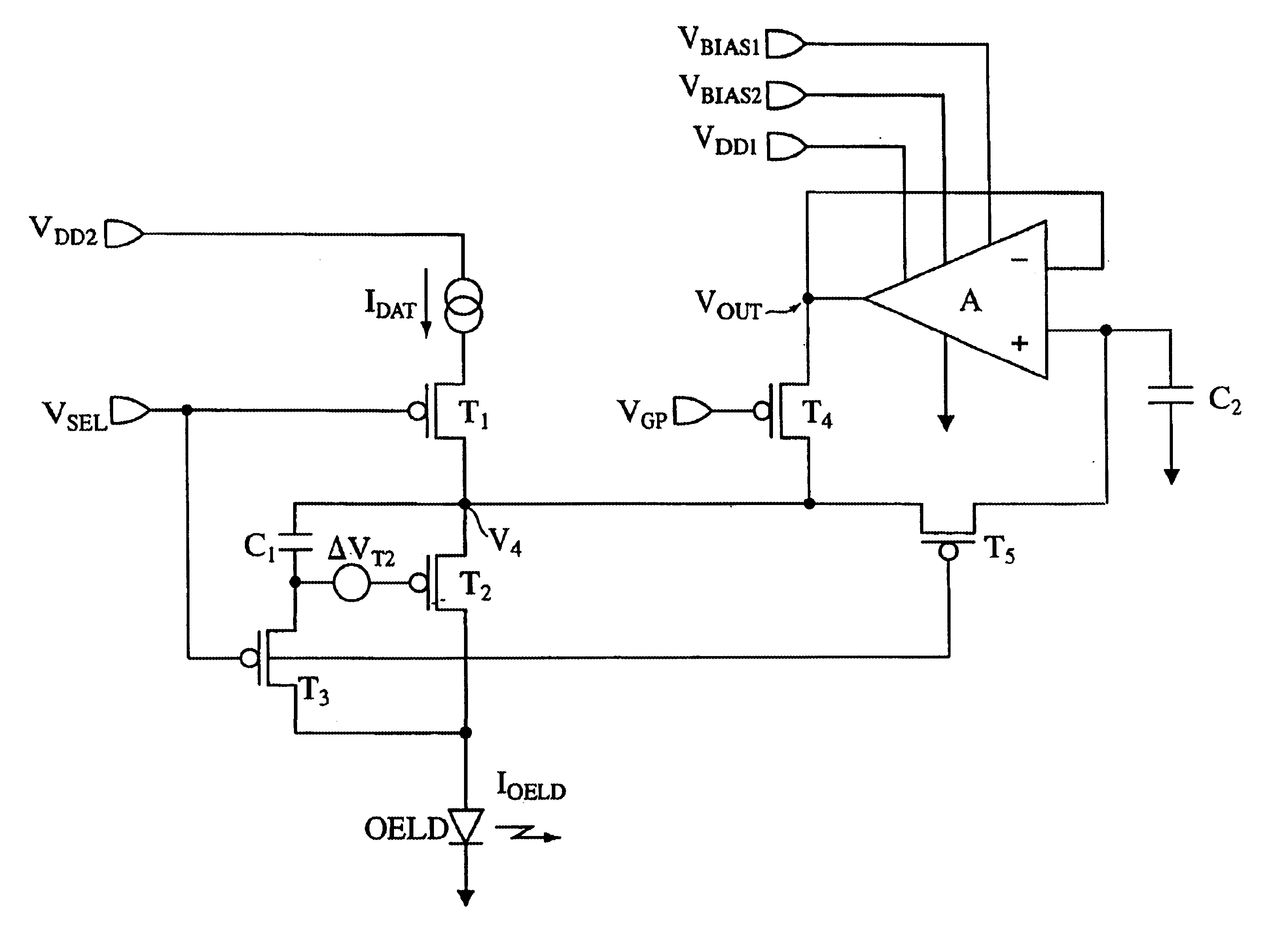
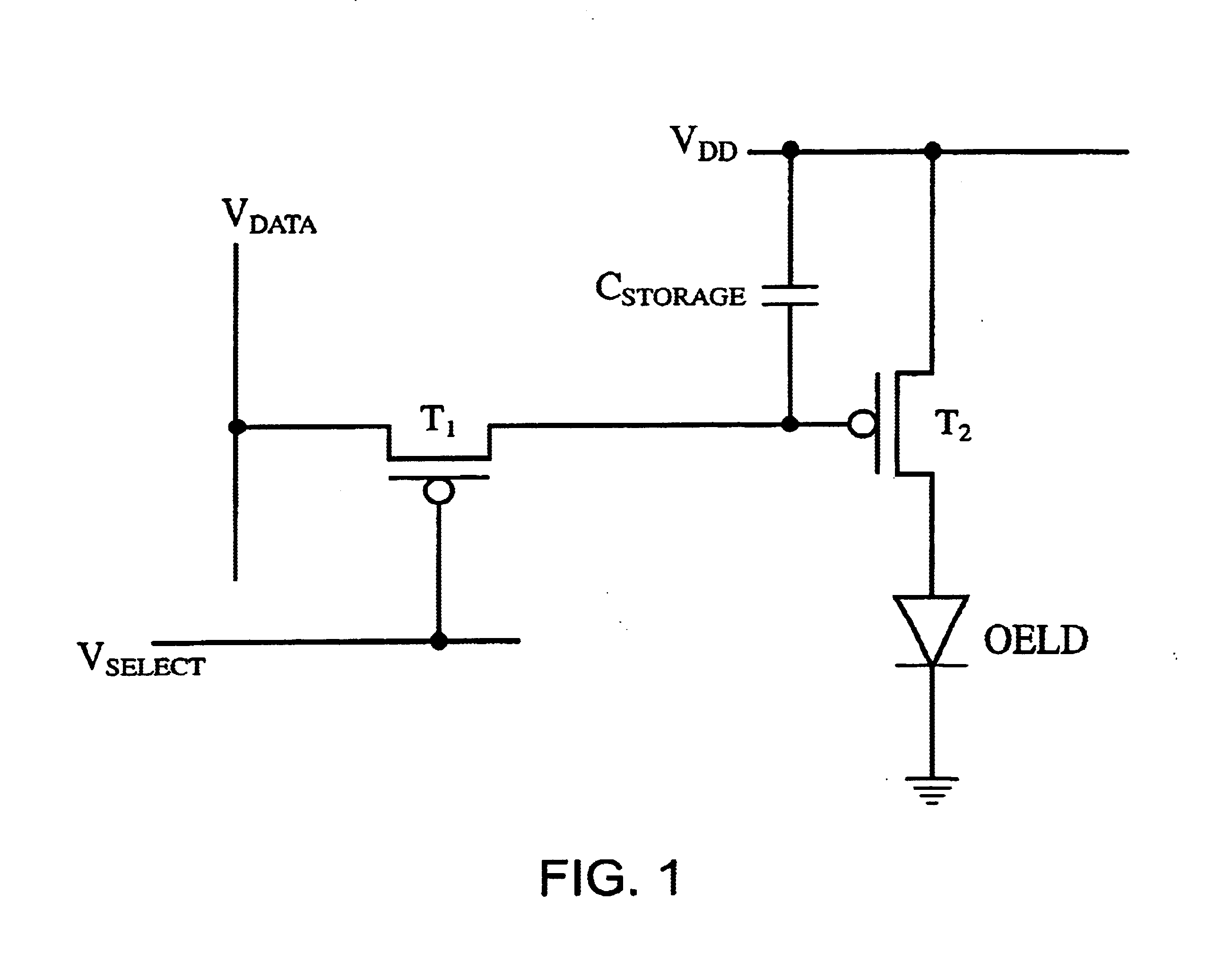
A compensated pixel driver circuit according to an embodiment of the present invention is shown in FIG. 3. Compared with the circuit of FIG. 2, there is added an operational amplifier OpAmp A, a capacitor C2 and a transistor T5. As shown in FIG. 3, Vout of the OpAmp is connected to the inverting input V_ thereof. The OpAmp thus has unity gain. Capacitor C2 ensures a sample ad hold function and transistor T5 acts as a control switch to store the voltage on C2. In effect the circuit provides a self-adjusted load or voltage source (VDD) and by thus holding the operative voltage constant the effect of the slope in the output characteristics can be avoided. In it's generic form, the OpAmp A is a unity gain buffer having it's input connected to the source-drain path of transistor T5 and it's output connected to the source-drain path of transistor T4, the input being connected to ground via capacitor C2.

As shown in FIG. 3, a TFT operational amplifier configured as a sample and hold circuit...


PUM


Abstract

A compensated pixel driver circuit for an organic electroluminescent device, wherein the circuit comprises a unity gain buffer which is preferably implemented as an operational amplifier. The circuit provides a unity gain sample and hold function, thereby compensating the current supply to the electroluminescent element by providing a self adjusting load.

Description

BACKGROUND OF THE INVENTION1. Field of the InventionThe present invention relates to an organic electroluminescent device and particularly to a compensated pixel driver circuit thereof.2. Description of Related ArtAn organic electro-luminescent device (OELD) consists of a light emitting polymer (LEP) layer sandwiched between an anode layer and a cathode layer. Electrically, this device operates like a diode. Optically, it emits light when forward biased and the intensity of the emission increases with the forward bias current. It is possible to construct a display panel wide a matrix of OELDs fabricated on a transparent substrate and with one of the electrode layers being transparent. One can also integrate the driving circuit on the same panel by using low temperature polysilicon thin film transistor (TFT) technology.In a basic analog driving scheme for an active mat OELD display, a minimum of two transistors are required per pixel (FIG. 1): T1 is for addressing the pixel and T2 is...

Claims


Application Information

Patent Timeline
Patent Type & Authority Patents(United States)
IPC IPC(8): G09G3/32
CPCG09G3/325G09G2300/0852G09G2300/0417
Inventor TAM, SIMON
Owner SEIKO EPSON CORP
Why Eureka
Try Eureka