
Liquid crystal display

a liquid crystal display and pentile matrix technology, applied in static indicating devices, non-linear optics, instruments, etc., can solve the problems of difficult to form the storage capacity required for the liquid crystal display, the limit of the pentile matrix pixel arrangement structure to the large-sized liquid crystal display, and the wiring line. achieve excellent display capacity

Inactive Publication Date: 2005-02-01
SHENZHEN CHINA STAR OPTOELECTRONICS TECH CO LTD
View PDF6 Cites 117 Cited by
  • Summary
  • Abstract
  • Description
  • Claims
  • Application Information

AI Technical Summary

Benefits of technology

It is an object of the present invention to provide a thin film transistor array substrate for a liquid crystal display which involves excellent display capacity while preventing the signal lines at the neighboring pixels from being short-circuited.
It is another object of the present invention to provide a thin film transistor array substrate for a liquid crystal display which involves excellent display capacity while securing the required amount of storage capacity in a stable manner.
It is still another object of the present invention to provide a thin film transistor array substrate for a liquid crystal display which involves excellent display capacity while being minimized in the substrate size with repair lines for repairing possible cutting or short-circuiting of the wiring lines.

Problems solved by technology

Therefore, there is a limit in applying the Pentile Matrix pixel arrangement structure to the large-sized liquid crystal display.
This makes it very difficult to form storage capacity required for the liquid crystal display.
Meanwhile, the data signal lines for transmitting data signals to the red or green pixels, or two gate signal lines are placed close to each other so that the wiring lines are liable to be short-circuited while reducing the production yield and deteriorating the display characteristic.
Furthermore, as the neighboring blue pixels are driven by one driving IC, the data driving IC should be provided at both sides of the display region and this induces enlargement of the display device.
In addition, with this structure, it becomes difficult to form repair lines at the periphery of the display region.
However, in this case, polarity is non-uniformly made with respect to the red, green and blue pixels while generating flicker as well as brightness difference among the pixel columns.
This deteriorates the picture quality of the resulting display device.

Method used


Image

  • Liquid crystal display
  • Liquid crystal display
  • Liquid crystal display

Examples


Embodiment Construction

Preferred embodiments of this invention will be explained with reference to the accompanying drawings.

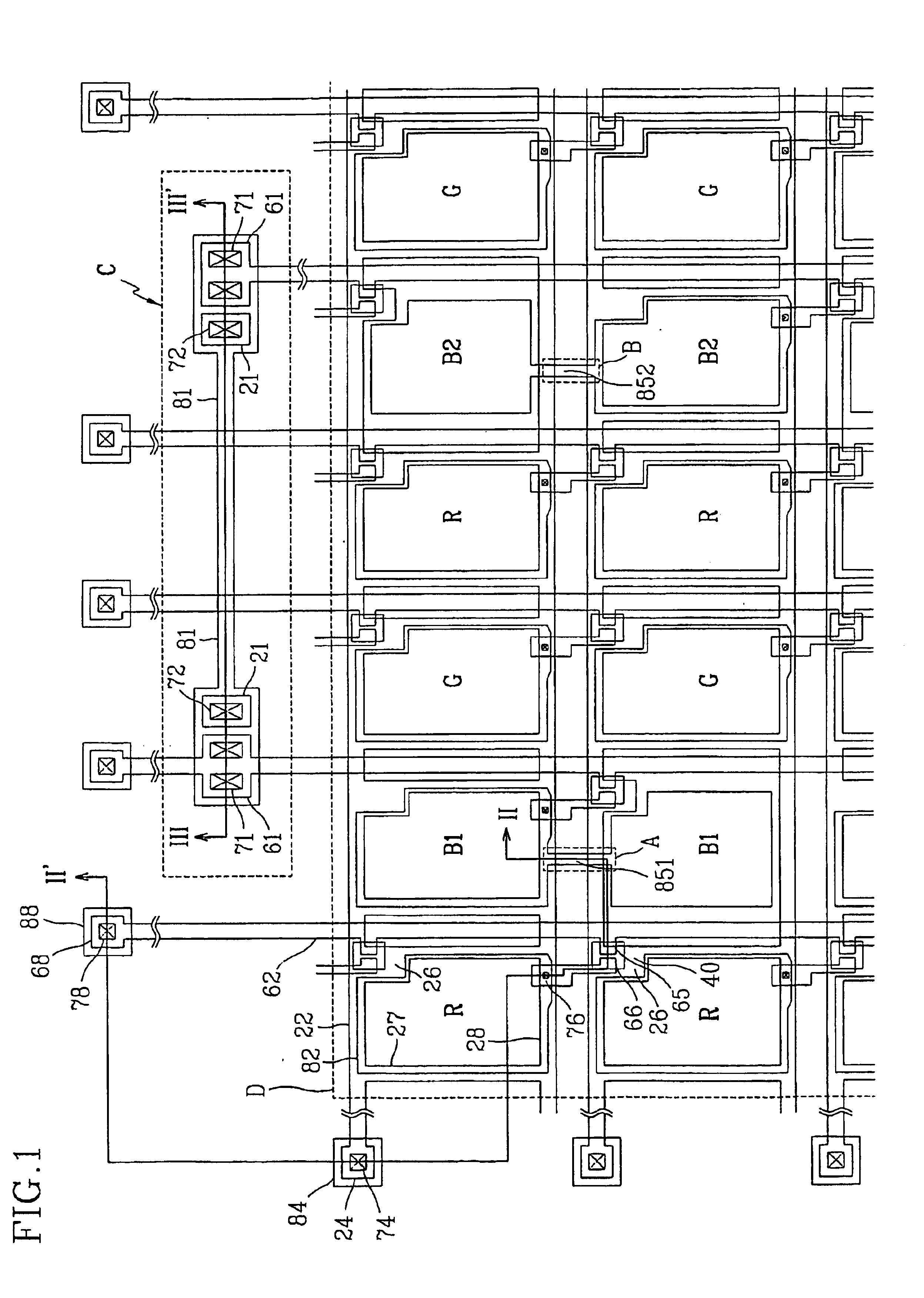
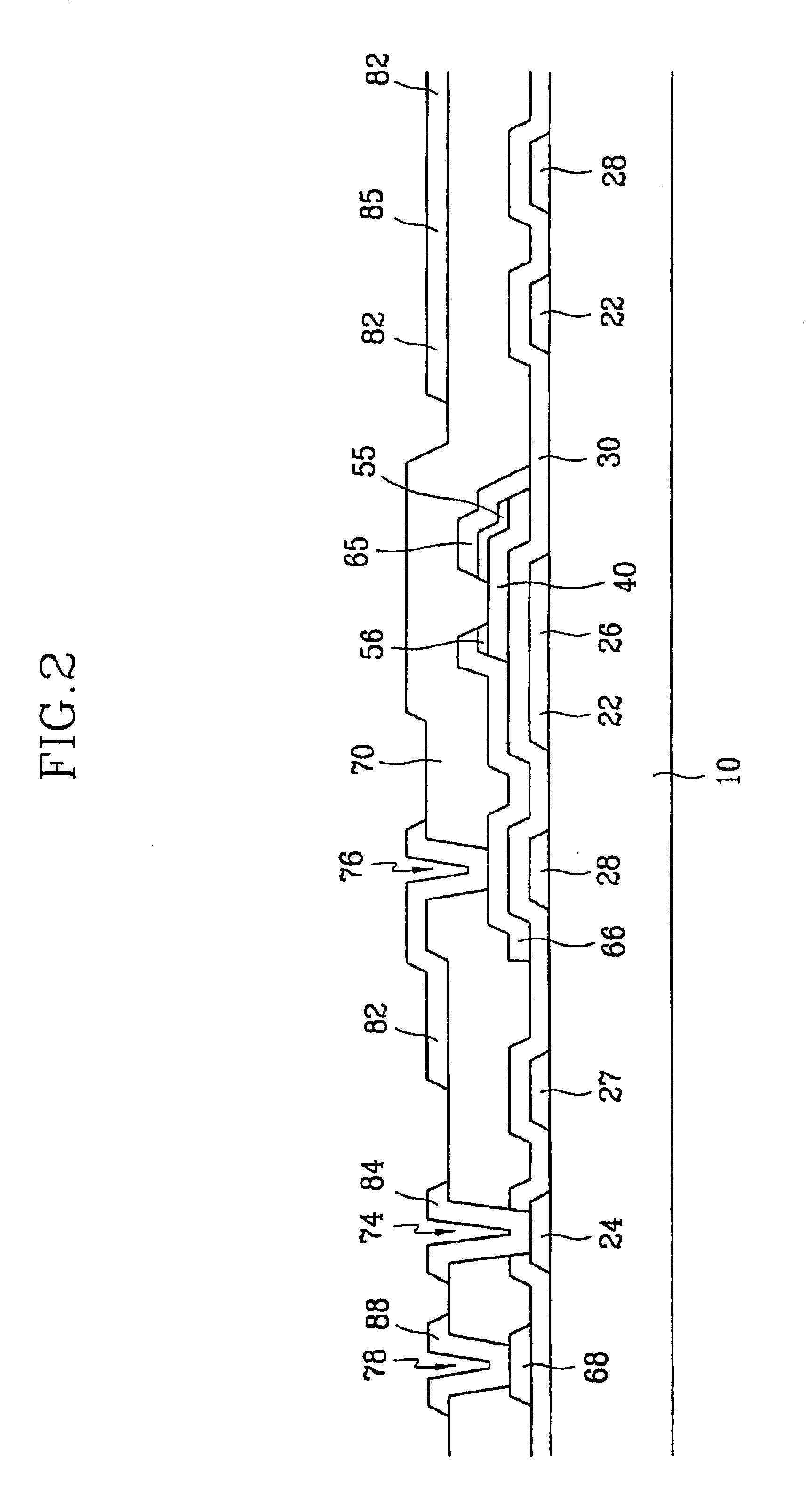
FIG. 1 is a plan view of a thin film transistor array substrate for a liquid crystal display according to a first preferred embodiment of the present invention, and FIGS. 2 and 3 are cross sectional views of the thin film transistor array substrate taken along the II-II′ line and the III-III′ line of FIG. 1. FIG. 2 specifically illustrates the pixel area and the pad area. FIG. 3 illustrates a connection unit C for interconnecting the data lines for transmitting data signals to the neighboring blue pixels B1 and B2 by way of one pad.

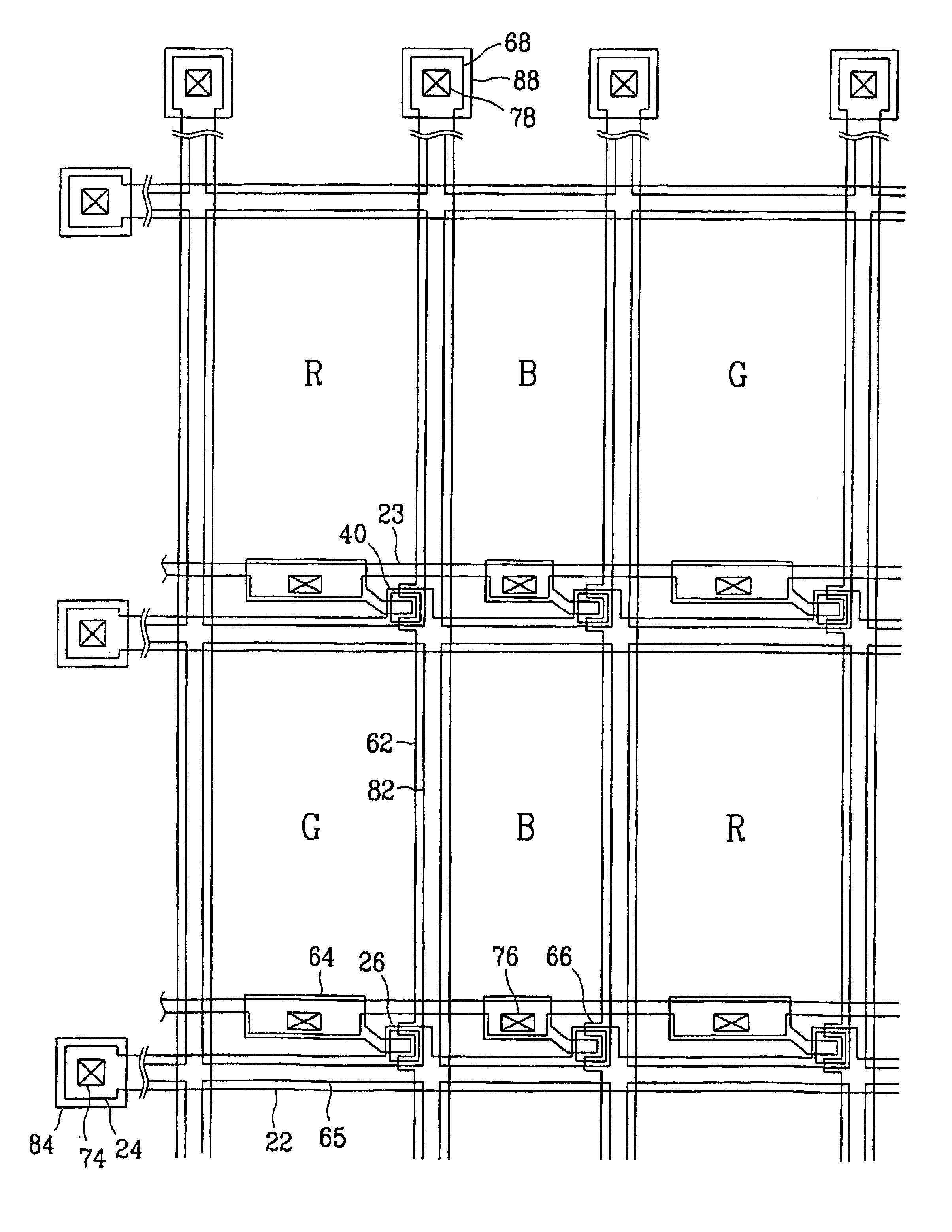
As shown in FIG. 1, pixels of red, blue and green R, B1, G, R, B2, and G are arranged in a matrix form at the thin film transistor array substrate. The red, blue and green pixels R, B1, G, R, B2 and G are sequentially arranged in the row direction with the same color pixel neighbors in the column direction. Alternatively, the red and green pixels R and G ...


PUM


Abstract

Pixels of red, blue and green are sequentially arranged in the row. The red and green pixels are alternately arranged in the column while the blue pixels being repeatedly arranged in the column. The four red and green pixels surrounding the two blue pixels at the two neighboring pixel rows face each other around the blue pixels. Gate lines are arranged at the respective rows to transmit scanning signals. Data lines cross over the gate lines in an insulating manner, and are arranged at the respective columns to transmit picture signals. Pixel electrodes and thin film transistor are formed at respective pixels. The blue pixel has the same area as or an area smaller than the red and green pixels. The pixel electrodes are overlapped with the gate or the data lines via a passivation layer of low dielectric organic material or an insulating material such as SiOC, SiOF.

Description

BACKGROUND OF THE INVENTION(a) Field of the InventionThe present invention relates to a liquid crystal display and, more particularly, to a liquid crystal display which involves a Pentile Matrix pixel arrangement structure for displaying picture images at high resolution.(b) Description of the Related ArtGenerally, a liquid crystal display has two substrates with electrodes, and a liquid crystal layer sandwiched between the two substrates. Voltages are applied to the electrodes so that the liquid crystal molecules in the liquid crystal layer are re-oriented to thereby control the light transmission.The liquid crystal display has a plurality of pixels with pixel electrodes and color filters of red, green and blue. The pixels are driven by way of signals applied through the wiring lines. The wiring lines include scanning signal lines or gate lines for carrying scanning signals, and picture signal lines or data lines for carrying the picture signals. Thin film transistors are formed at...

Claims


Application Information

Patent Timeline
IPC IPC(8): G02F1/1335G02F1/13G02F1/13357G02F1/133G02F1/1343G02F1/1345G02F1/1368
CPCG02F1/133514G09G3/3614G02F2201/52G02F1/133
Inventor ROH, NAM-SEOKHONG, MUN-PYOCHAI, CHONG-CHULRHO, SOO-GUY
Owner SHENZHEN CHINA STAR OPTOELECTRONICS TECH CO LTD
Learn More