Semiconductor device and method of manufacturing the same

Inactive Publication Date: 2005-02-08
RENESAS ELECTRONICS CORP
View PDF14 Cites 88 Cited by
  • Summary
  • Abstract
  • Description
  • Claims
  • Application Information

AI Technical Summary

Benefits of technology

(i) In the semiconductor device manufacturing method, there is used a wiring substrate on which plural product forming areas are arranged longitudinally and transversely in regular order, and semiconductor chips are fixed respectively to the product forming areas through an adhesive, but in this fixing step the adhesive which has protruded enters the groove and does not flow out beyond the groov

Problems solved by technology

In the semiconductor device manufacturing method which adopts the above block molding method there is a problem that voids are apt to be formed at corner portions defined by side faces of the chip and a main surface of the substrate.
It has newly been found out that various problems arise in case of forming a semiconductor device by the above block molding method and if an attempt is made to adopt a conventional means for preventing the contamination of electrodes on a wiring substrate caused by

Method used


Image

  • Semiconductor device and method of manufacturing the same
  • Semiconductor device and method of manufacturing the same
  • Semiconductor device and method of manufacturing the same

Examples


first embodiment

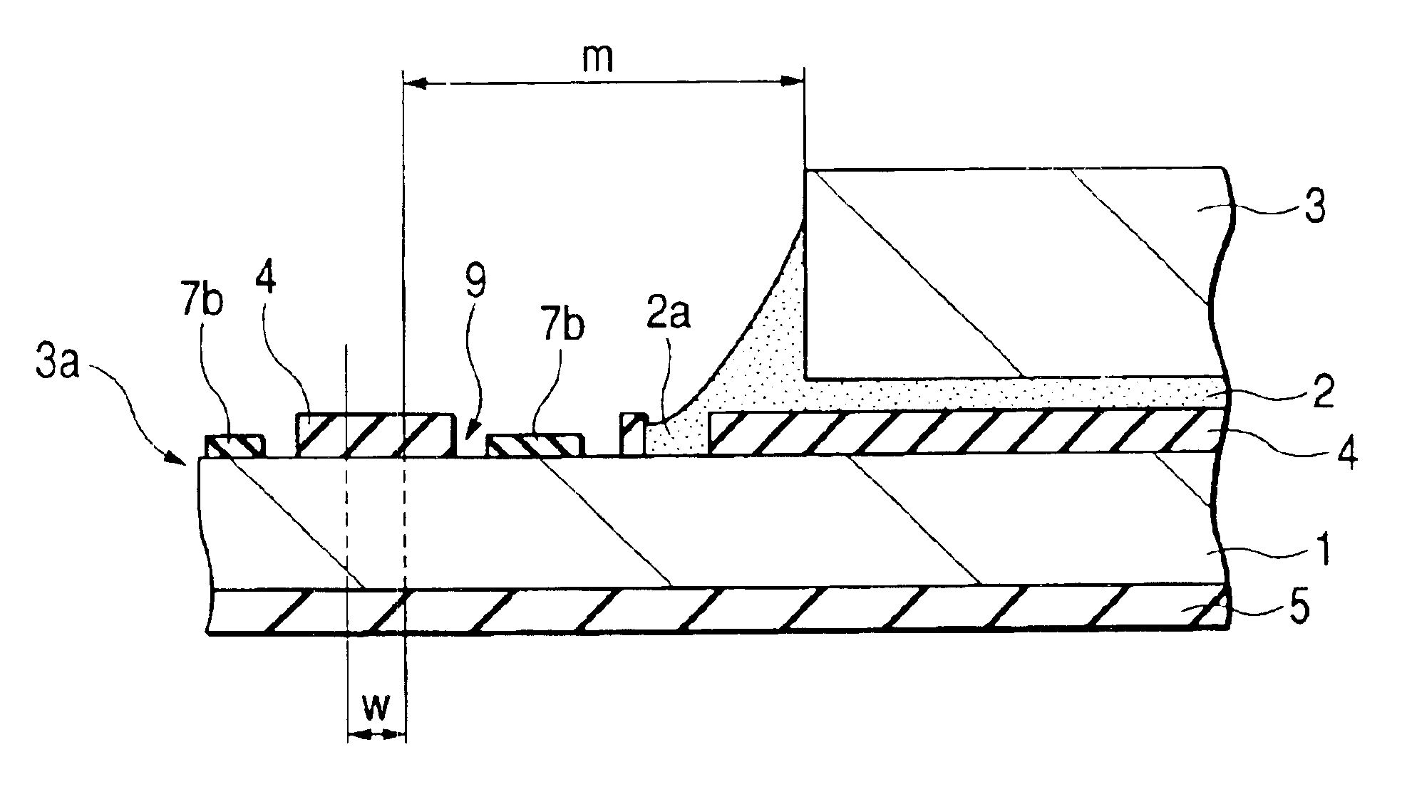
FIGS. 1 to 25 illustrate an MAP type semiconductor device and a method of manufacturing the same according to an embodiment (first embodiment) of the present invention. In the first embodiment the present invention is applied, though not specially limited, to a memory semiconductor device with two semiconductor chips mounted side by side thereon, the semiconductor chips each constituting a 64 MDRAM. FIGS. 1 to 7 are concerned with a structure of the semiconductor device, while FIGS. 8 to 25 are concerned with a method of manufacturing the semiconductor device.

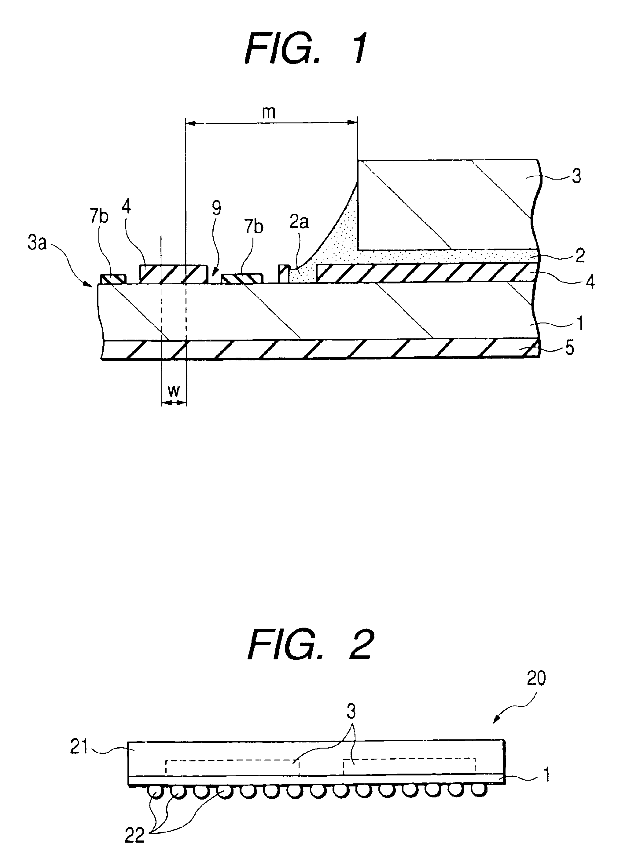
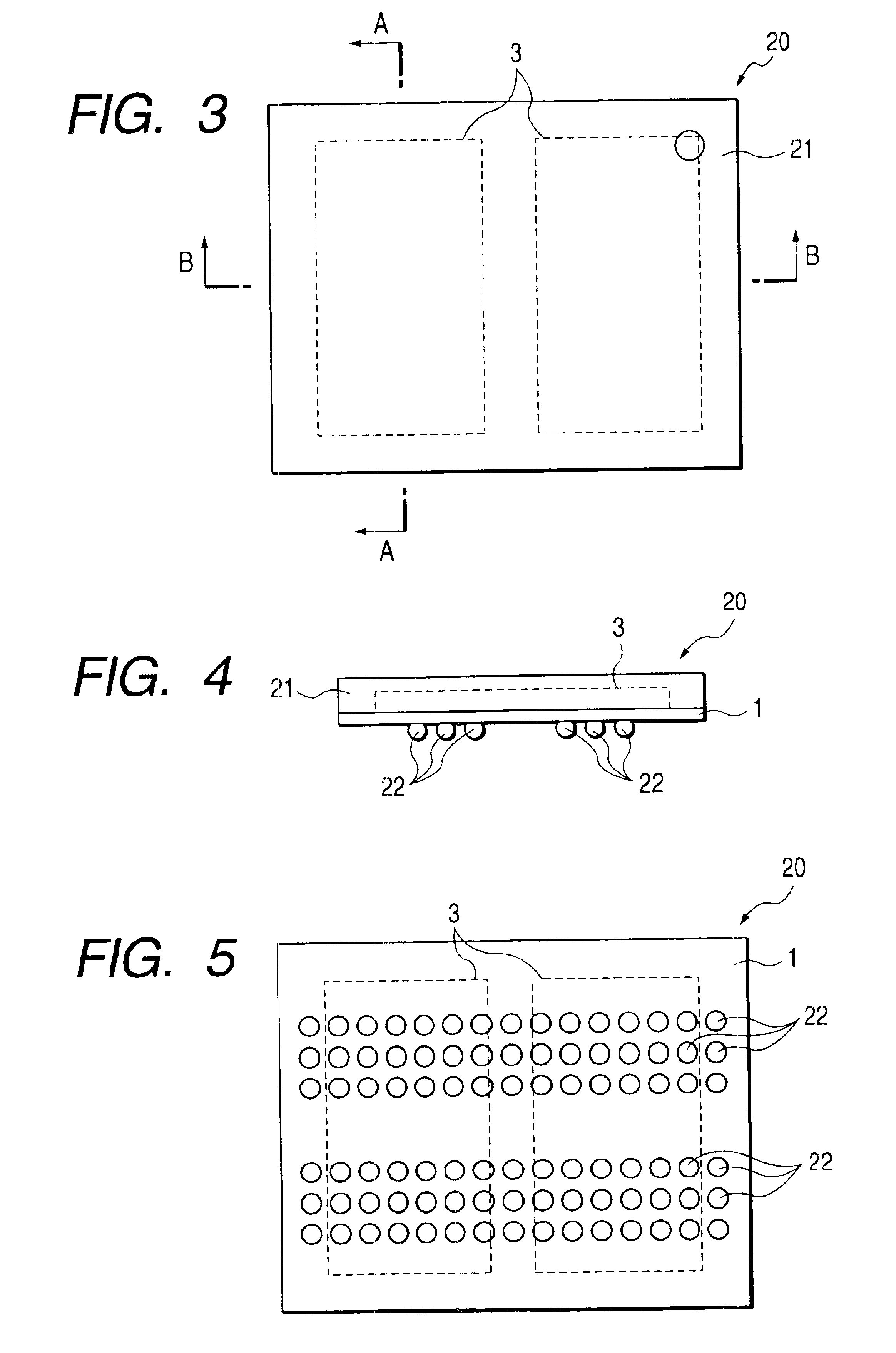
The semiconductor device of the first embodiment is of such a structure as shown in FIGS. 2 to 7, of which FIGS. 2, 3, 4, and 5 are a front view, a plan view, a side view, and a bottom view, respectively, of the semiconductor device, FIG. 6 is an enlarged sectional view taken along line A—A in FIG. 3, and FIG. 7 is an enlarged sectional view taken along line B—B in FIG. 3.

As shown in FIGS. 2 to 5, the semiconductor device 20 co...

second embodiment

FIGS. 26 and 27 are concerned with a method of manufacturing a semiconductor device according to another embodiment (second embodiment) of the present invention, of which FIG. 26 is a plan view showing a main surface of a product forming area on a substrate which is used in the manufacture of the semiconductor device and FIG. 27 is a plan view showing the main surface of the product forming area with semiconductor chips mounted thereon.

In the semiconductor device manufacturing method according to this second embodiment, grooves 25 are also formed along long sides of each product forming area 31. To be more specific, in the first embodiment grooves 25 are formed outside and along the long sides of each chip mounting area 34, while in this second embodiment grooves 25 are also formed outside and along the short sides of each chip mounting area. The grooves 25 formed on both long and short sides are not in direct contact with each other.

Each semiconductor chip 3 is quadrangular (see FI...

third embodiment

FIGS. 28 and 29 are concerned with a method of manufacturing a semiconductor device according to a further embodiment (third embodiment) of the present invention, of which FIG. 28 is a plan view showing a main surface of a product forming area on a substrate which is used in the manufacture of the semiconductor device and FIG. 29 is a plan view of the main surface of the product forming area with semiconductor chips mounted thereon.

In this third embodiment, a groove 25 is formed so as to surround the whole periphery of each chip mounting area 34 in the pattern of the product forming area 31 described in the first embodiment. In this third embodiment, a pasty material gets into the groove formed around the whole periphery of the chip concerned at the time of chip bonding. This brings about an effect of controlling the crawling-up of the pasty material onto the chip and controlling the protrusion of the pasty material from side faces of the chip.


PUM


Abstract

In the manufacture of a semiconductor device by adopting a block molding method wherein a semiconductor chip is fixed onto a wiring substrate through an adhesive, the occurrence of a defect caused by flowing-out of the adhesive is to be prevented. The semiconductor device according to the present invention comprises a wiring substrate, the wiring substrate having a main surface, an insulating film formed on the main surface, and electrodes formed on the main surface so as to be exposed from the insulating film, a semiconductor chip fixed through an adhesive onto the insulating film formed on the main surface of the wiring substrate, conductive wires for connecting the electrodes on the main surface of the wiring substrate and electrodes on the semiconductor chip with each other, and a seal member, i.e., a package, which covers the semiconductor chip, the main surface of the wiring substrate and the electrodes, wherein a groove is formed between the semiconductor chip and the electrodes and the seal member and the wiring substrate have side faces cut by dicing. A protruding portion of the adhesive (an insulating resin) stays within the groove without getting over the groove and does not reach the electrodes. The groove is formed by removing the insulating film partially in the full depth direction of the film so as to extend through the film.

Description

BACKGROUND OF THE INVENTIONThe present invention relates to a semiconductor device and a method of manufacturing the same. Particularly, the present invention is concerned with a technique effectively applicable to a method (MAP: Matrix Array Packaging method) which involves block-molding a main surface side of a wiring board (substrate) with an insulating resin to cover the main surface side with a seal member, or a package, and thereafter dividing the mutually superimposed substrate and seal member longitudinally and transversely to afford plural semiconductor devices.In semiconductor devices incorporated into small-sized electronic devices such as portable telephones, portable information processing terminal devices, and portable personal computers, it is required to reduce the thickness and size and attain a multi-pin structure. As package forms of semiconductor devices adapted for such a multi-function and high density configuration there are known such package structures as BG...

Claims


Application Information

Patent Timeline
IPC IPC(8): H01L21/56H01L21/02H01L21/60H01L23/48H01L21/58H01L23/498H01L23/12H01L23/28
CPCH01L21/56H01L21/561H01L23/49838H01L24/06H01L24/27H01L24/32H01L24/743H01L24/83H01L24/97H01L24/29H01L24/45H01L2221/68331H01L2224/04042H01L2224/05599H01L2224/06136H01L2224/27013H01L2224/32225H01L2224/45144H01L2224/48091H01L2224/48227H01L2224/48235H01L2224/49171H01L2224/73265H01L2224/743H01L2224/83051H01L2224/83192H01L2224/83194H01L2224/83385H01L2224/8385H01L2224/85399H01L2224/92H01L2224/97H01L2924/01002H01L2924/01004H01L2924/01005H01L2924/01006H01L2924/01047H01L2924/01074H01L2924/01079H01L2924/014H01L2924/07802H01L2924/0781H01L2924/15311H01L24/48H01L2224/2919H01L2924/01019H01L2924/01033H01L2924/0665H01L24/49H01L2924/00014H01L2924/12041H01L2224/48599H01L2224/29011H01L2224/26175H01L2224/05554H01L2224/83H01L2224/85H01L2224/92247H01L2924/00H01L2924/00012H01L2924/3512H01L24/73H01L2924/10161H01L2924/181H01L23/28
Inventor UJIIE, MIKAKOSUGIYAMA, MICHIAKISUZUKI, KAZUNARIMASUDA, MASACHIKAWADA, TAMAKI
Owner RENESAS ELECTRONICS CORP
Why Eureka
Try Eureka