Liquid crystal display device

Inactive Publication Date: 2005-02-08
UNIFIED INNOVATIVE TECH
View PDF13 Cites 32 Cited by
  • Summary
  • Abstract
  • Description
  • Claims
  • Application Information

AI Technical Summary

Benefits of technology

The provision of the first and second inspection circuits on the liquid crystal display substrate enables, before unitization of the liquid crystal display device, inspection of breaks in the data lines, short circuits between adjacent data lines, breaks in the scanning lines, short circuits

Problems solved by technology

A main method of inspecting this liquid crystal display substrate is a method of touching probe pins to ends of each vertical and horizontal lines of the matrix, which needs a large number of probe pins, leading to an expensive inspecting apparatus.
Therefore, the liquid crystal display substrate is subjected to perform display in its

Method used


Image

  • Liquid crystal display device
  • Liquid crystal display device
  • Liquid crystal display device

Examples


first embodiment

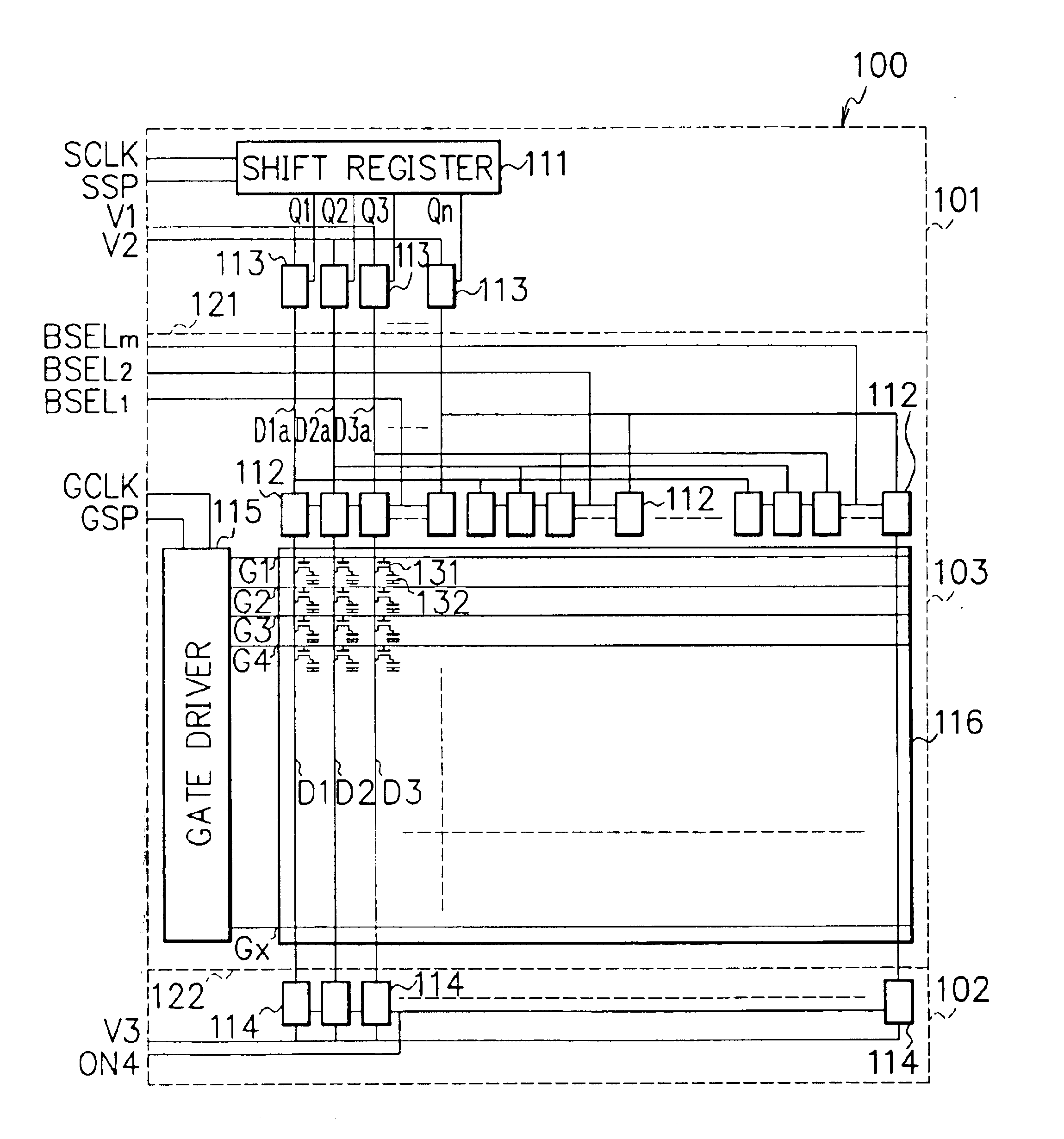
FIG. 1 shows a liquid crystal display substrate 100 according to the first embodiment of the present invention. A first inspection circuit 101, a display circuit 103, and a second inspection circuit 102 are provided on one glass substrate 100. The first inspection circuit 101 is separable from the display circuit 103 at a cutting line 121. The second inspection circuit 102 is separable from the display circuit 103 at a cutting line 122.

The display circuit 103 has a gate driver 115, a pixel region 116 and analog switches 112. The gate driver 115 is connected to the pixel region 116 through scanning lines G1 to Gx to supply scanning signals to the scanning lines G1 to Gx in response to gate clocks GCLK and gate start pulses GSP.

The pixel region 116 has TFTs 131 and liquid crystal capacitors 132 which are arranged in a two-dimensional matrix. The TFTs 131 are n-channel MOS transistors, of which gates are connected to the scanning lines G1 to Gx, drains are connected to data lines D1 to...

second embodiment

FIG. 5 shows the liquid crystal display substrate 100 according to the second embodiment of the present invention. The second embodiment differs from the first embodiment in that the second inspection circuit is included in the display circuit 103 and signal lines V3 and V4 are alternately connected to the other ends of the input / output terminals of the analog switches 114, and the other points are the same.

Different inspection signals are inputted to the signal lines V3 and V4 for operation at the timing in FIG. 3 as in the first embodiment. In this event, if, for example, the data lines D1 and D2 short-circuit to each other, or the data lines D1a and D2a short-circuit to each other, the same signal is detected in the signal lines V1 and V2. On the other hand, if the data lines D1 and D2 do not short-circuit to each other and the data lines D1a and D2a do not short-circuit to each other, the inspection signal inputted to the signal line V3 is detected in the signal line V1, and the...

third embodiment

FIG. 6 shows the liquid crystal display substrate 100 according to the third embodiment of the present invention. The third embodiment differs from the second embodiment in that n-channel MOS transistors 601 and capacitors (condensers) 602 are provided, and the other points are the same.

In the transistors 601, gates are connected to the scanning lines G1 to Gx respectively, drains are connected to a common signal line Vmon, and sources are connected to a common voltage terminal via the capacitors 602.

FIG. 7 is a timing chart showing the inspection method. The gate driver 115 outputs the scanning signals sequentially to the scanning lines G1 to Gx in response to clocks GCLK and start pulse GSP. During a period 701 of the output, an inspection voltage Va is inputted to the signal line Vmon. The transistors 601 turn on when the scanning lines G1 to Gx are set to the high level respectively to store the inspection voltage Va in the capacitors 602.

Next, the start pulse GSP is inputted ag...


PUM


Abstract

A liquid crystal display device includes a display circuit having data lines and scanning lines arranged in two-dimensional matrix, and switching elements connected between the data lines and the scanning lines. A first inspection circuit is also provided, including an inspection voltage input and/or output terminal for inputting and/or outputting an inspection voltage to/from one ends of the data lines via a first analog switch. A second inspection circuit includes an inspection voltage input and/or output terminal for inputting and/or outputting an inspection voltage to/from the other ends of the data lines. The display circuit, the first inspection circuit, and the second inspection circuit are provided on one substrate, and the first inspection circuit is constructed to be separated from the rest of the display circuit.

Description

CROSS-REFERENCE TO RELATED APPLICATIONSThis application is based upon and claims priority of Japanese Patent Application No. 2001-101176, filed on Mar. 30, 2001, the contents being incorporated herein by reference.BACKGROUND OF THE INVENTION1. Field of the InventionThe present invention relates to a liquid crystal display device and, more specifically, to a liquid crystal display device with switching elements connected to data lines and scanning lines.2. Description of the Related ArtFIG. 26 shows a structure of a liquid crystal display substrate according to the prior art. A data driver (data line driver) 5 is connected to a pixel region 7 via data lines 3. A gate driver (scanning line driver) 6 is connected to the pixel region 7 via scanning lines 4. The data driver 5 can supply data to the data lines 3. The gate driver 6 can supply scanning signals to the scanning lines 4.The pixel region 7 has switching elements (TFTs: Thin Film Transistors) 1 and liquid crystal capacitors 2 wh...

Claims


Application Information

Patent Timeline
IPC IPC(8): G09G3/36G01R31/02G02F1/13G02F1/1345G02F1/1368G09F9/00G09F9/30
CPCG09G3/3688G09G2300/0408G02F1/1345
Inventor KAI, TSUTOMUOKAZAKI, SUSUMUZHANG, HONGYONGOHASHI, NORIYUKI
Owner UNIFIED INNOVATIVE TECH
Why Eureka
Try Eureka