Method and apparatus for forming a cavity in a semiconductor substrate using a charged particle beam

a technology of semiconductor substrate and charged particle beam, which is applied in the direction of electrical apparatus, basic electric elements, electric discharge tubes, etc., can solve the problems of large-scale bulk silicon removal that would take too long using the ion beam, large surface defects on the backside of the die surface, and large surface defects, etc., to achieve slow etching and less aggressive

Inactive Publication Date: 2005-02-15
CREDENCE SYSTEMS
View PDF7 Cites 11 Cited by
  • Summary
  • Abstract
  • Description
  • Claims
  • Application Information

AI Technical Summary

Benefits of technology

Hence, as disclosed here, first any anti-reflective coating present on the substrate surface in which the trench is to-be formed is locally removed. Then an “unassisted etch” process (this is an FIB milling process with no injected gas) is used to smooth the entire exposed substrate surface. If the scratches or pits are deep, the FIB is defocused. During that time, typically, as a result a Ga+ (gallium ion) implanted layer is formed from the FIB Ga+ ions at the exposed surface. Next, this implanted layer is removed using the FIB with an injected gas but not using the same gas as used later to etch the trench proper but instead a less aggressive gas (slower etching), such as EDI (ethylene-di-iodide). This gas is selected as it is less aggressive against the substrate crystalline material than the gas used later for the actual trench etching and thus exposes the substrate surface without any overetch. This less aggressive gas etching step provides a smooth (defect free) surface in which to commence the actual FIB etching of the trench. The effect of this local cleaning process is observed in real time by an associated infra-red optical microscope or similar optical observation system which in one embodiment is coaxial with the ion beam.

Problems solved by technology

Otherwise, if the trench floor is not perfectly flat (smooth) and contains, for instance, cavities such as scratches and pits, those scratches and pits will allow excess energy of the ion beam to penetrate therethrough and damage active regions (transistors) so as to not perform an accurate circuit edit.
Similar problems arise if the trench floor is overetched on one side.
These mechanical die thinning techniques are used because large scale bulk silicon removal would take too long using the ion beam.
These thinning processes are relatively cumbersome and also have been found to still leave significant surface defects in the backside die surface.
Hence, even with the prior art cumbersome milling or lapping process, the surface defects are still present which end up undesirably replicating themselves in the bottom of the trench, i.e., the trench floor.

Method used


Image

  • Method and apparatus for forming a cavity in a semiconductor substrate using a charged particle beam
  • Method and apparatus for forming a cavity in a semiconductor substrate using a charged particle beam
  • Method and apparatus for forming a cavity in a semiconductor substrate using a charged particle beam

Examples


Embodiment Construction

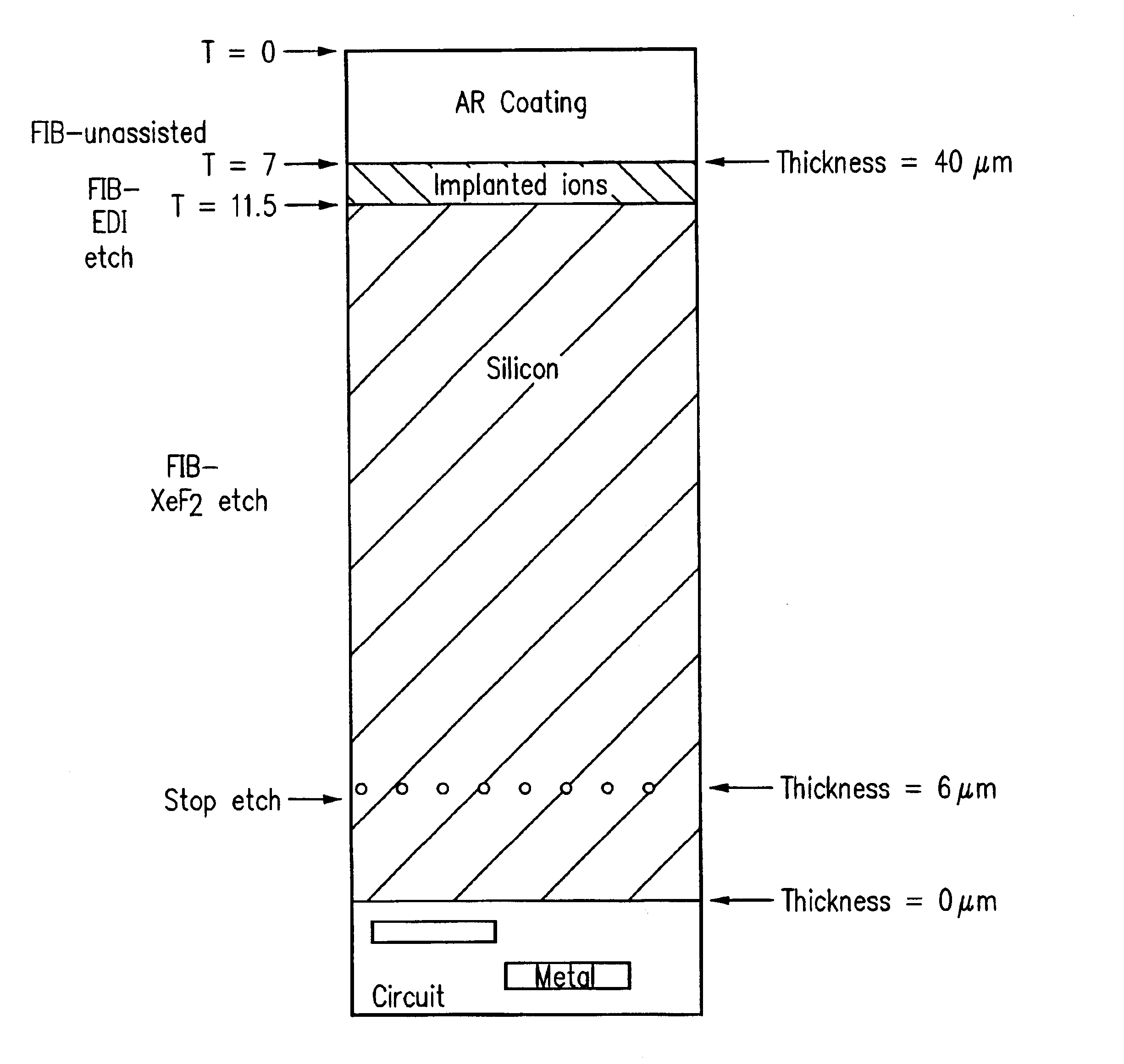
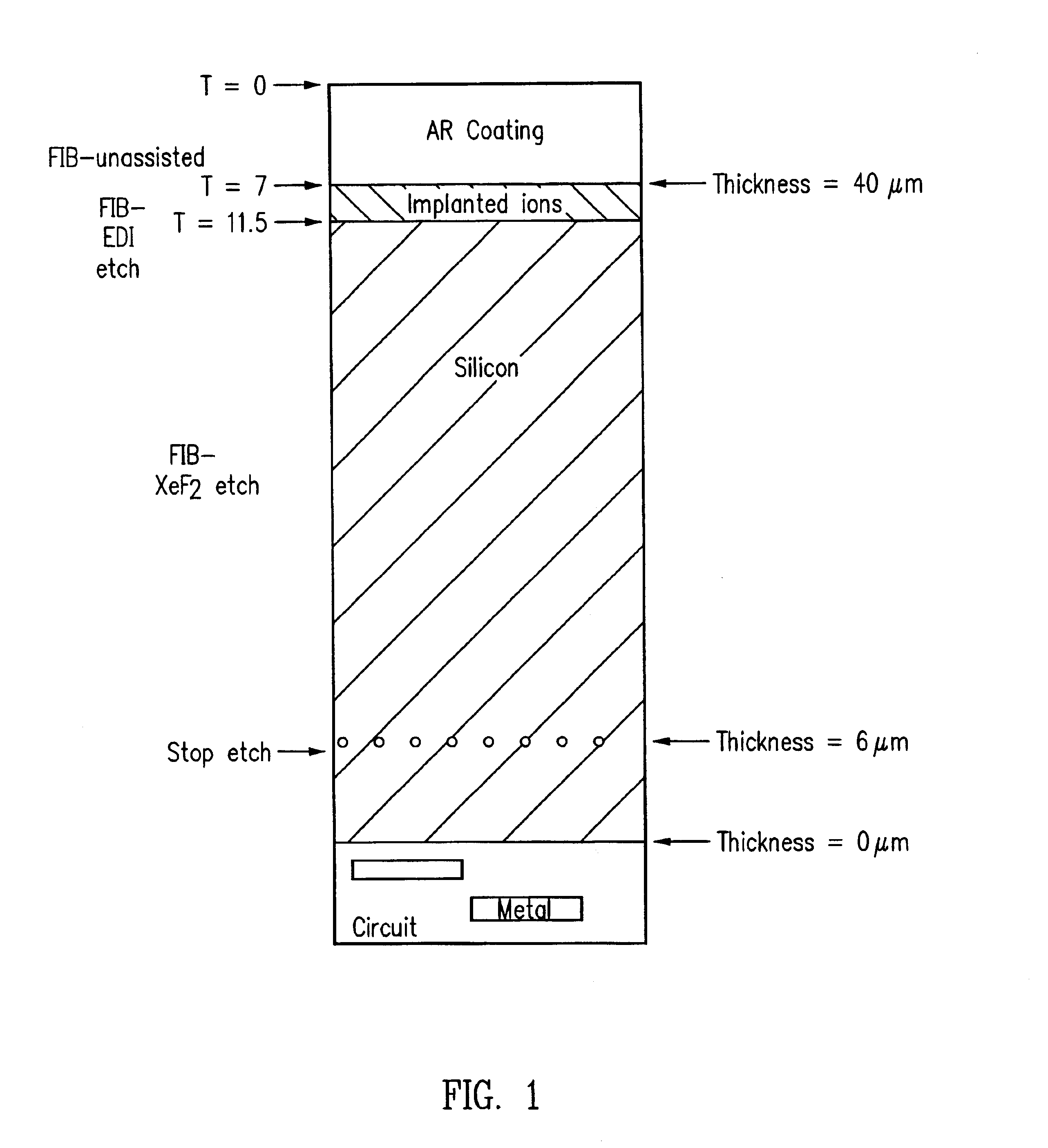
For detail of an FIB apparatus system useful in accordance with this disclosure, see, e.g., U.S. Pat. Nos. 6,225,626 and 5,140,164. Conventional detail of this apparatus and the accompanying well known FIB techniques for forming trenches is not included herein except as shown in FIGS. 6a, 6b. Briefly, however, the FIB tool (apparatus) includes a source of (e.g., gallium) ions, an XY movable stage which moves the FIB column under the integrated circuit under test, a Z stage for adjusting the working distance of the workpiece to the FIB column so as to adjust the focus of the light optical column and for holding the workpiece which is typically an integrated circuit from which the packaging has been at least partly removed (or was never packaged), suitable vacuum enclosures and controls, the FIB column which accelerates and focuses the ions onto the workpiece, and conventional apparatus for injecting “chemistry” gas into the FIB under controlled circumstances to enhance the FIB etchin...


PUM


Abstract

Apparatus and method for exposing a selected feature of an integrated circuit device such as a selected portion of the metallization layer, from the backside of the integrated circuit substrate without disturbing adjacent features of the device such as the active semiconductor regions. This is performed using an FIB (focused ion beam) etching process in conjunction with observation by an optical microscope to form a trench through the substrate. The floor of the trench is formed so as to be as smooth and planar as possible, thereby preventing undesirable exposure of the underlying active regions through any unknown or undesired cavity caused by scratches or pits or a deeper than desired sidewall. The smoothness and planarity of the floor of the trench is established by, prior to forming the trench, removing any surface defect initially present by using an FIB etching without use of assist gas to eliminate most scratches or impurities on the surface of the silicon, followed by removal of implanted ions using a gas-injected assisted FIB etch. Then the actual trench is formed using an assisted etch using a more aggressive injected gas.

Description

FIELD OF THE INVENTIONThis disclosure pertains to semiconductor technology and more specifically to forming a trench through a semiconductor substrate so as to access, from the backside of the substrate, interconnection metal layers formed on the opposing principal surface of the substrate, the trenching process using a focused ion beam.DESCRIPTION OF THE PRIOR ARTIt is well known to use a focused ion beam (FIB) for exposing conductors on an integrated circuit (IC) to aid in debug, or failure analysis, and repair of the integrated circuit. See for instance U.S. Pat. No. 6,225,626, issued May 1, 2001, to Talbot et al.; U.S. Pat. No. 5,140,164, issued Aug. 18, 1992 to Talbot et al.; and U.S. Pat. No. 5,616,921, issued Apr. 1, 1997 to Talbot et al., all incorporated herein by reference in their entireties. U.S. Pat. No. 6,225,626 discloses methods for exposing a selected feature of an IC such as a selective conductor, from the backside of the IC substrate without disturbing adjacent fe...

Claims


Application Information

Patent Timeline
Patent Type & Authority Patents(United States)
IPC IPC(8): H01L21/02H01L21/263H01L21/311H01L21/3065H01L21/265H01J37/30H01J37/305
CPCH01J37/228H01J37/3005H01J37/3056H01L21/31105H01L21/2633H01L21/3065H01J2237/2482H01J2237/30455H01J2237/3174H01J2237/31744H01L21/26506H01J2237/31737
Inventor LE ROY, ERWANTHOMPSON, MARK A.
Owner CREDENCE SYSTEMS
Why Eureka
Try Eureka