Etching system and method of manufacturing semiconductor device
a semiconductor device and etching system technology, applied in the direction of basic electric elements, electrical equipment, electric discharge tubes, etc., can solve the problems of difficult control of etching a layer or film into a controlled shape, or desired shape, and achieve the effect of easy control of the shap
- Summary
- Abstract
- Description
- Claims
- Application Information
AI Technical Summary
Benefits of technology
Problems solved by technology
Method used
Image

Examples
first embodiment
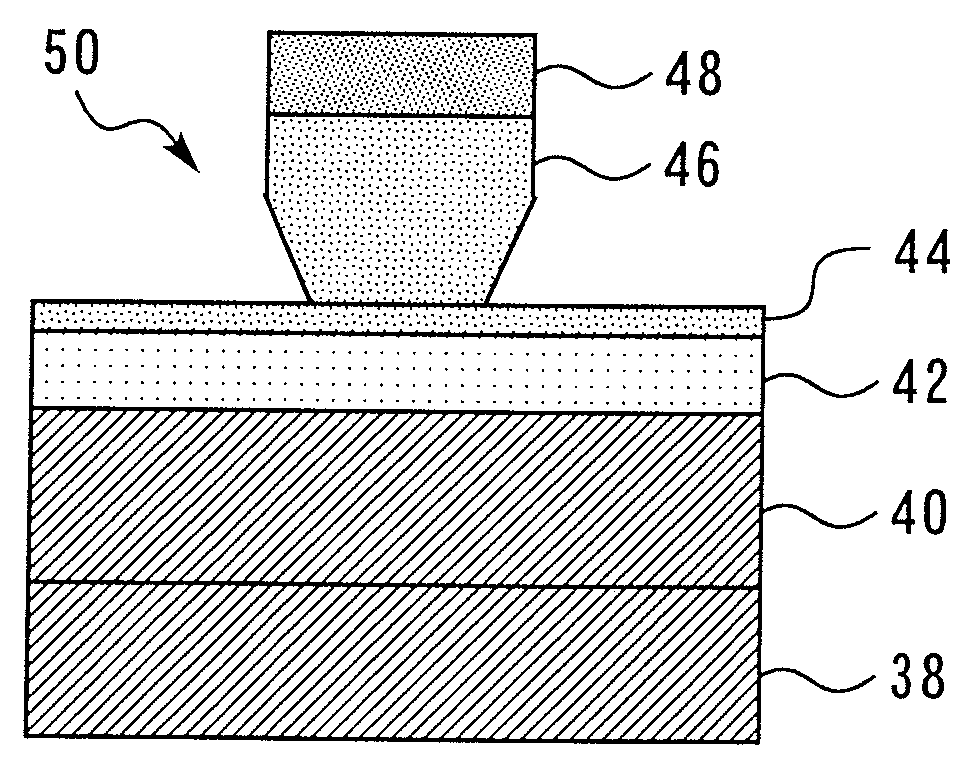
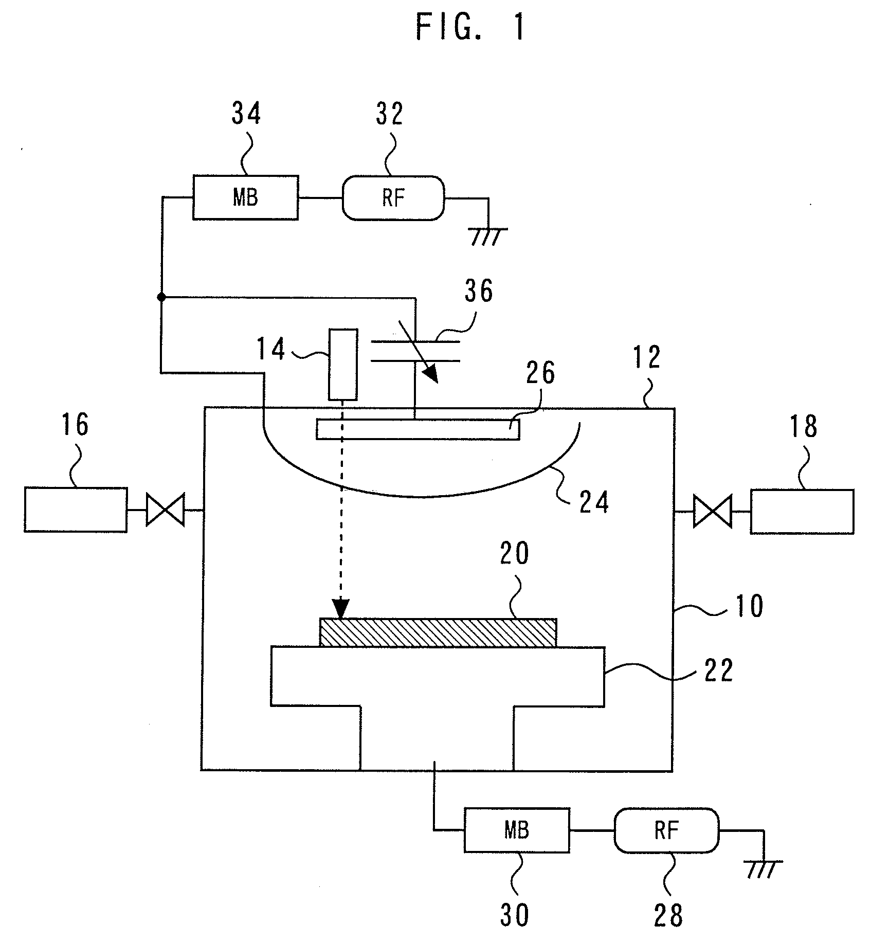
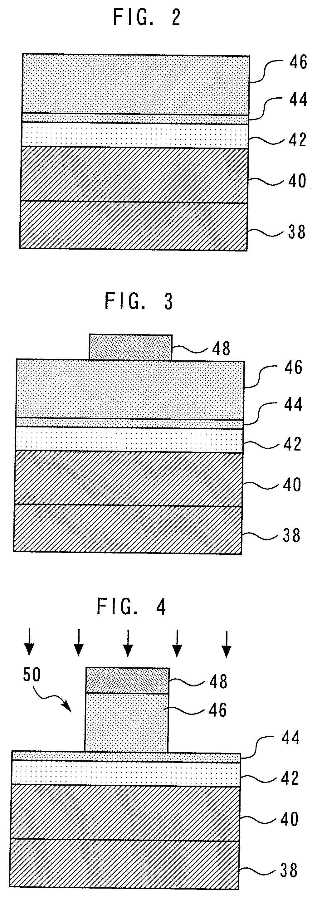
[0017]FIG. 1 is a diagram showing an etching system according to a first embodiment of the present invention. In FIG. 1, a vacuum chamber 10 is shown whose ceiling 12 is made of transparent quartz glass. A laser beam interferometric end point detector 14 is provided in the ceiling 12 of the vacuum chamber 10. The vacuum chamber 10 is also provided with gas supply means 16 and gas evacuation means 18 to introduce a process gas into and to evacuate the chamber 10, respectively.
[0018]The vacuum chamber 10 contains a stage 22 for mounting a workpiece 20 thereon and also contains an ICP electrode 24 (referred to in the appended claims as a “first electrode”) disposed above the stage 22. Between the ICP electrode 24 and the ceiling 12 of the vacuum chamber 10 is disposed a planar electrode 26 (referred to in the appended claims as a “second electrode”) including a plurality of radially extending antennas.
[0019]A radio frequency power supply 28 is connected to the stage 22 through a matchi...
second embodiment
[0030]FIG. 10 is a diagram showing an etching system according to a second embodiment of the present invention. This etching system differs from that of the first embodiment in that the variable capacitor 36 is replaced by a variable capacitance element made up of a plurality of parallel-connected fixed capacitances 52a, 52b, and 52c and a plurality of switches 54a, 54b, and 54c connected in series to the capacitances 52a, 52b, and 52c, respectively. All other components are the same as in the first embodiment. That is, the total capacitance of the variable capacitance element can be varied by selectively switching the switches 54a, 54b, and 54c, resulting in the same advantages as described above in connection with the first embodiment.
third embodiment
[0031]FIG. 11 is a diagram showing an etching system according to a third embodiment of the present invention. This etching system is constructed as follows. A radio frequency power supply 32 (referred to in the appended claims as a “first radio frequency power supply”) is connected to the ICP electrode 24 through a matching box 34, and a radio frequency power supply 56 (referred to in the appended claims as a “second radio frequency power supply”) is connected to the planar electrode 26 through a matching box 58. The radio frequency power supplies 28, 32, and 56 supply RF power to the stage 22, the ICP electrode 24, and the planar electrode 26, respectively, thereby producing inductively coupled plasmas from the process gas within the vacuum chamber 10. Other components perform the same functions as those described in connection with the first embodiment. This arrangement allows the workpiece 20 to be etched into a controlled shape by varying the RF power supplied from the radio fr...
PUM
| Property | Measurement | Unit |
|---|---|---|
| Power | aaaaa | aaaaa |
| Capacitance | aaaaa | aaaaa |
Abstract
Description
Claims
Application Information
 - R&D Engineer
- R&D Manager
- IP Professional
- Industry Leading Data Capabilities
- Powerful AI technology
- Patent DNA Extraction
Browse by: Latest US Patents, China's latest patents, Technical Efficacy Thesaurus, Application Domain, Technology Topic.
© 2024 PatSnap. All rights reserved.Legal|Privacy policy|Modern Slavery Act Transparency Statement|Sitemap