Precise patterning of high-K films

a high-k film, precise technology, applied in the direction of basic electric elements, electrical apparatus, semiconductor devices, etc., can solve the problems of inability to control the depth of the trench, undesirable undercutting neighboring structures,

Inactive Publication Date: 2005-02-15
INTEL CORP
View PDF5 Cites 29 Cited by
  • Summary
  • Abstract
  • Description
  • Claims
  • Application Information

AI Technical Summary

Benefits of technology

Microelectronic structures, such as semiconductor structures, may be created by forming layers and trenches in various structural configurations from various materials. One of the challenges associated with conventional techniques utilized for patterning dielectric films, such as high dielectric constant, or “high-K”, films is trenching with accuracy to avoid damage to the integrity of adjacent structures. Referring to FIG. 1A, a cross-sectional view of a typical gate structure is depicted wherein two gates (104, 106) with spacers (108, 110, 112, 114) are formed adjacent a high-K gate oxide layer (102), which is formed adjacent a substrate layer (100). FIG. 1B depicts an undesirable patterning scenario wherein dry etching techniques have been utilized, resulting in a trench (116) that is overdeep. While the relatively anisotropic properties of dry etching techniques are favored for minimizing negative etch bias, they may be associated with difficulty in controlling trenching depth, as depicted, for example, in FIG. 1B, where the trench (116) extends undesirably into the substrate layer (100). FIG. 1C depicts another undesirable patterning scenario wherein wet etching has been utilized, resulting in a trench (118) that undesirably undercuts neighboring structures such as gates (104, 106) and spacers (110, 112). Many wet etching treatments are associated with substantially isotropic etch rate characteristics, resulting in negative etch bias and undercutting, as depicted, for example, in FIG. 1C.

Problems solved by technology

One of the challenges associated with conventional techniques utilized for patterning dielectric films, such as high dielectric constant, or “high-K”, films is trenching with accuracy to avoid damage to the integrity of adjacent structures.
While the relatively anisotropic properties of dry etching techniques are favored for minimizing negative etch bias, they may be associated with difficulty in controlling trenching depth, as depicted, for example, in FIG. 1B, where the trench (116) extends undesirably into the substrate layer (100). FIG. 1C depicts another undesirable patterning scenario wherein wet etching has been utilized, resulting in a trench (118) that undesirably undercuts neighboring structures such as gates (104, 106) and spacers (110, 112).

Method used


Image

  • Precise patterning of high-K films
  • Precise patterning of high-K films
  • Precise patterning of high-K films

Examples


Embodiment Construction

In the following detailed description of embodiments of the invention, reference is made to the accompanying drawings in which like references indicate similar elements. The illustrative embodiments described herein are disclosed in sufficient detail to enable those skilled in the art to practice the invention. The following detailed description is therefore not to be taken in a limiting sense, and the scope of the invention is defined only by the appended claims.

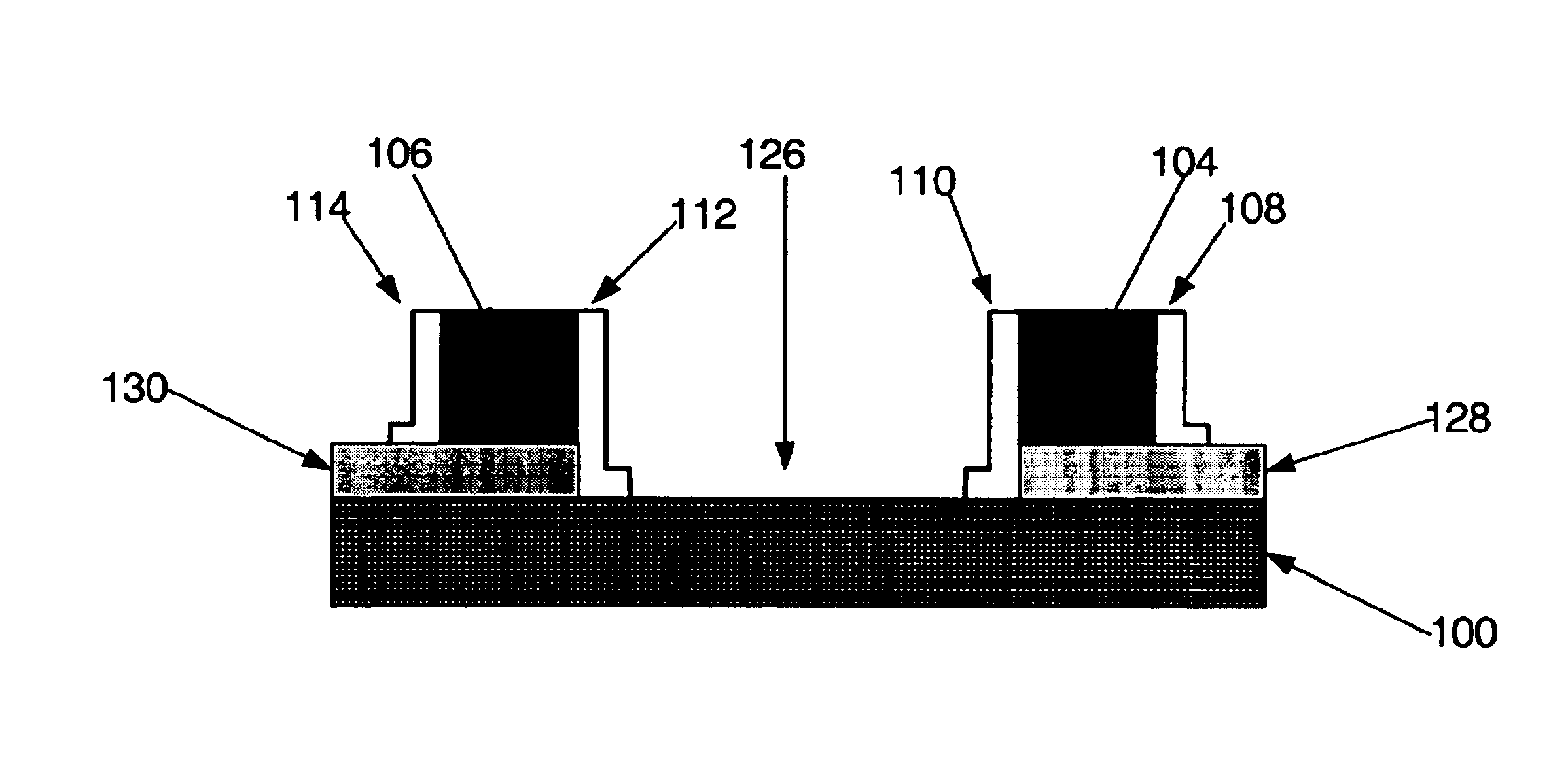
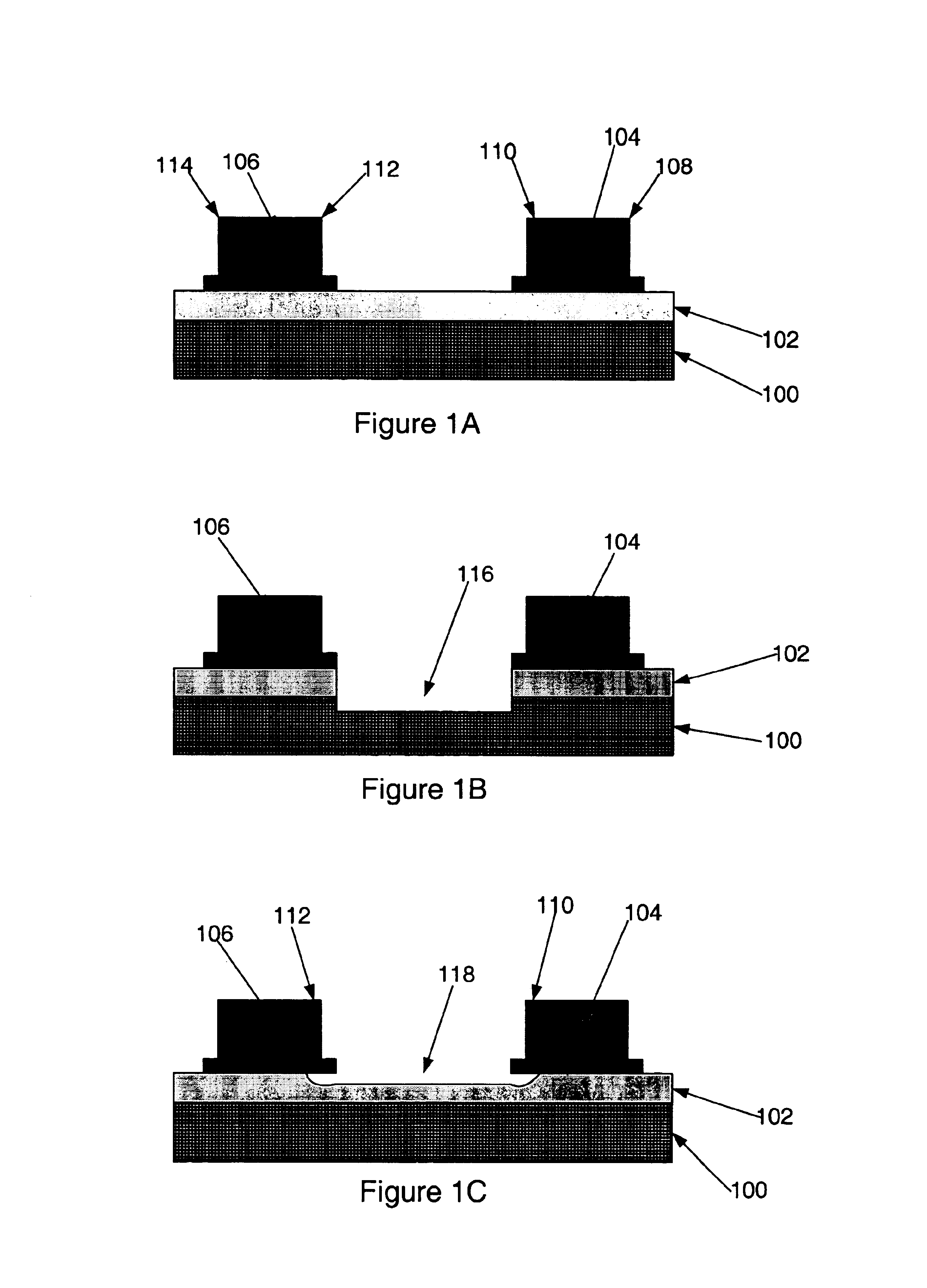
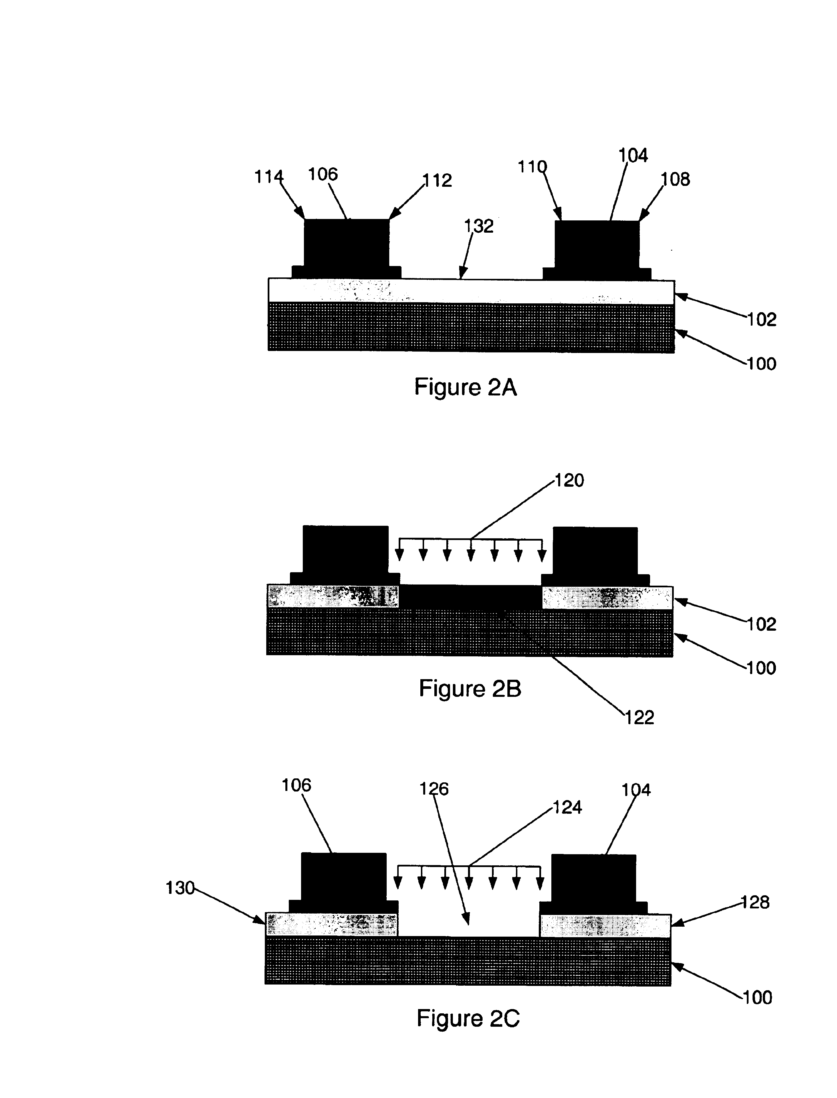
FIGS. 2A-2C are cross sectional views of various aspects of a patterning treatment of one embodiment of the present invention. Referring to FIG. 2A, a microelectronic structure similar to that depicted in FIG. 1A is shown. Such a structure may be formed utilizing various techniques and materials. For example, a high-K dielectric layer (102) may be formed upon a substrate layer (100) using techniques such as chemical or physical vapor deposition or other techniques. In various embodiments, the high-K dielectric layer (102) m...


PUM


Abstract

A high-K thin film patterning solution is disclosed to address structural and process limitations of conventional patterning techniques. Subsequent to formation of gate structures adjacent a high-K dielectric layer, a portion of the high-K dielectric layer material is reduced, preferably via exposure to hydrogen gas, to form a reduced portion of the high-K dielectric layer. The reduced portion may be selectively removed utilizing wet etch chemistries to leave behind a trench of desirable geometric properties.

Description

FIELD OF THE INVENTIONThis invention relates to fabricating microelectronic devices, and more particularly to precision formation of a trench in a dielectric layer.BACKGROUND OF THE INVENTIONMicroelectronic structures, such as semiconductor structures, may be created by forming layers and trenches in various structural configurations from various materials. One of the challenges associated with conventional techniques utilized for patterning dielectric films, such as high dielectric constant, or “high-K”, films is trenching with accuracy to avoid damage to the integrity of adjacent structures. Referring to FIG. 1A, a cross-sectional view of a typical gate structure is depicted wherein two gates (104, 106) with spacers (108, 110, 112, 114) are formed adjacent a high-K gate oxide layer (102), which is formed adjacent a substrate layer (100). FIG. 1B depicts an undesirable patterning scenario wherein dry etching techniques have been utilized, resulting in a trench (116) that is overdee...

Claims


Application Information

Patent Timeline
Patent Type & Authority Patents(United States)
IPC IPC(8): H01L21/02H01L21/28H01L21/3063H01L21/311
CPCH01L21/31111H01L21/28123H01L21/3063
Inventor BRASK, JUSTIN K.DOCZY, MARK L.METZ, MATTHEW V.BARNAK, JOHNMARKWORTH, PAUL R.
Owner INTEL CORP
Why Eureka
Try Eureka