Electromagnetic wave detector

a detector and electromagnetic wave technology, applied in the field of electromagnetic wave detectors, can solve the problems of adversely affecting the transistors and making them no longer work properly, and achieve the effect of effective and efficient detection of high-energy electromagnetic waves

Inactive Publication Date: 2005-02-15
CANON KK
View PDF15 Cites 8 Cited by
  • Summary
  • Abstract
  • Description
  • Claims
  • Application Information

AI Technical Summary

Benefits of technology

In view of the above circumstances, it is therefore an object of the present invention to provide an electromagnetic wave detector that operates more excellently than comparable known detectors and adapted to detect high energy electromagnetic waves effectively and efficiently.

Problems solved by technology

Then, the residual electric charge is added to the electric charge stored in the next cycle to give rise to a problem of after image when moving images are involved.
Additionally, if the storage capacitors are loaded excessively with electric charge, the excessive charge can leak out to the read circuit to give rise to a phenomenon like that of blooming in a CCD image sensor.
Additionally, when transistors for reading the stored electric charge are formed in a bulk by using a monocrystalline wafer, electric charges unintentionally generated by high energy electromagnetic waves in the bulk can adversely affect the transistors to make them no longer operate properly.

Method used


Image

  • Electromagnetic wave detector
  • Electromagnetic wave detector
  • Electromagnetic wave detector

Examples


Embodiment Construction

Now, an electromagnetic wave detector according to the invention will be described in greater detail by referring to FIGS. 1 to 2, 3A to 3C, 4A, 4B, 5 and 6 of the accompanying drawings that schematically illustrate preferred embodiments of the invention.

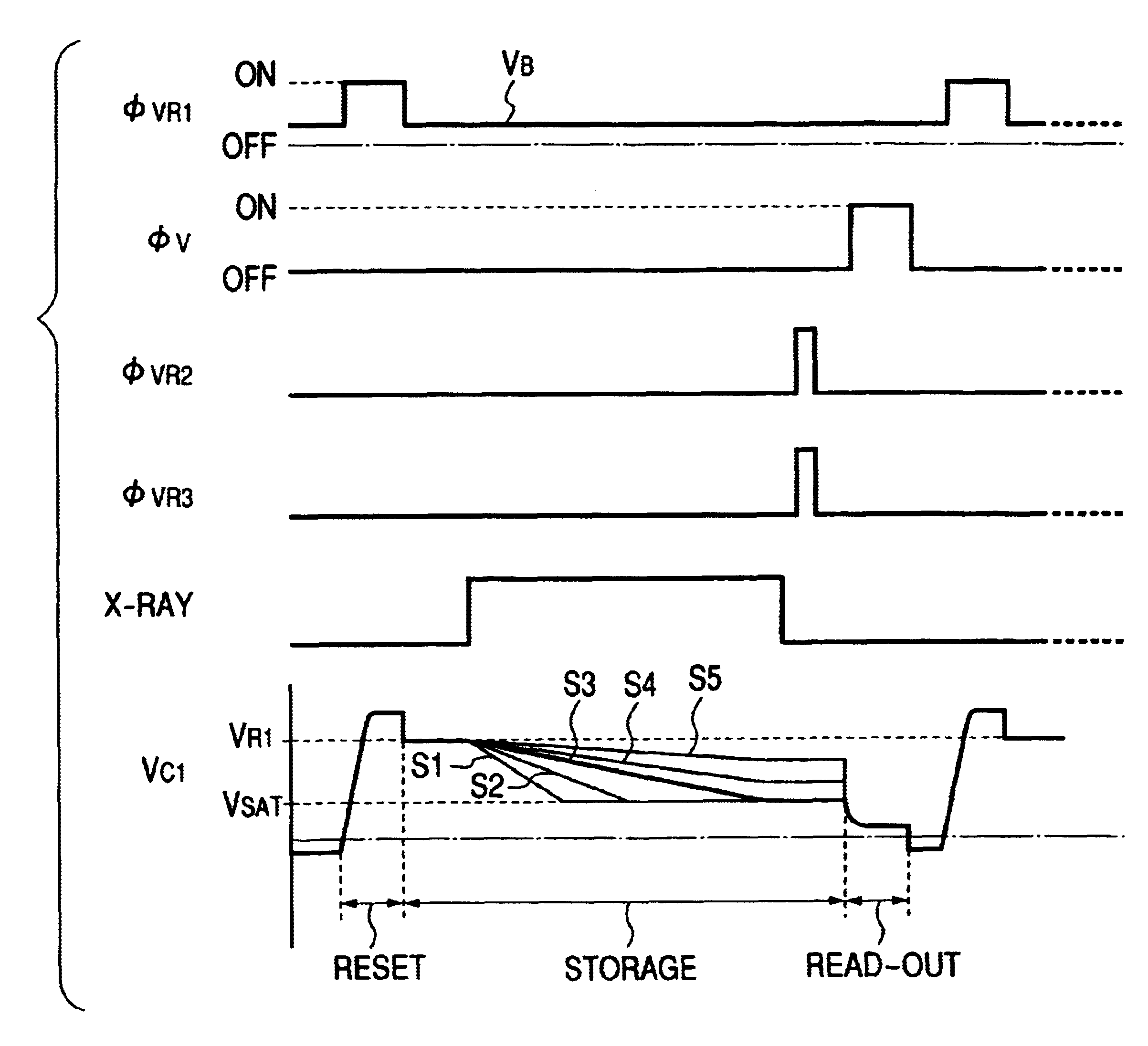
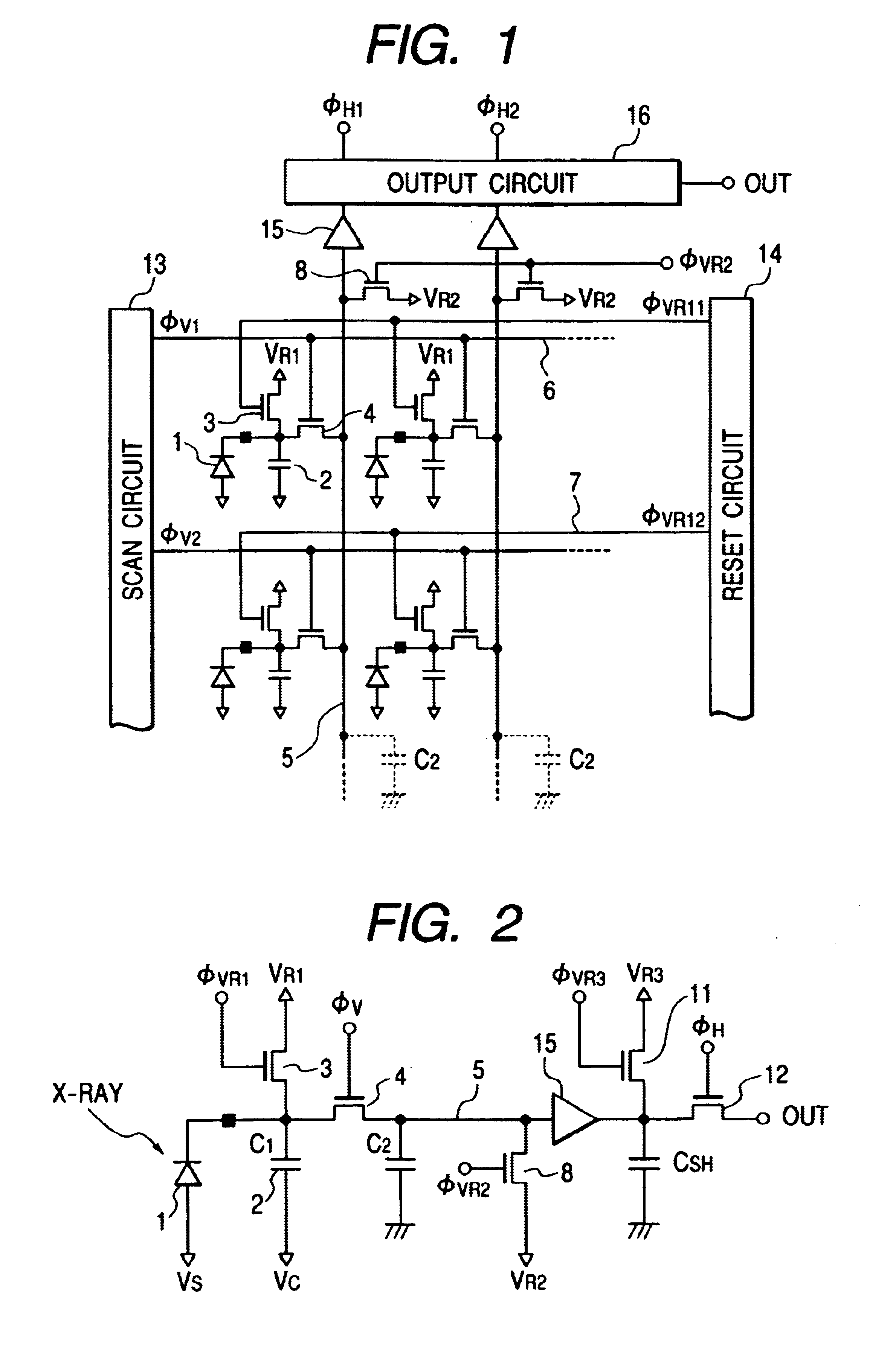
FIG. 1 is a schematic circuit diagram of an embodiment of electromagnetic wave detector according to the invention, showing its circuit configuration.

FIG. 2 is a schematic circuit diagram of part of the embodiment of electromagnetic wave detector of FIG. 1, including the output circuit for reading the signal of a unit cell.

Referring to FIGS. 1 and 2, reference numerals 1 and 2 respectively denote a conversion element and a storage capacitor and reference numerals 3 and 4 respectively denote a reset transistor and a read transistor, whereas reference numerals 5 and 6 respectively denote an output line and a horizontal drive control line and reference numerals 7 and 8 respectively denote a reset control line and a reset transistor of ...


PUM


Abstract

An electromagnetic wave detector includes a conversion element for converting incident electromagnetic waves or high energy radiations into an electric charge, a storage capacitor for storing the electric charge produced by the conversion element, a thin film read transistor connected to the storage capacitor, and a thin film reset transistor also connected to the storage capacitor. To the gates of the read and reset thin film transistors are applied ON and OFF voltages at predetermined timings and these voltages are set to values such that any excessive electric charge produced in the storage period is discharged by way of the thin film reset transistor, not by way of the thin film read transistor, in the same storage period.

Description

BACKGROUND OF THE INVENTION1. Field of the InventionThis invention relates to an electromagnetic wave detector for detecting electromagnetic waves or high energy radiations such as ultraviolet rays, infrared rays, rays of visible light, X rays, α rays or γ rays.2. Related Background ArtElectromagnetic wave detectors adapted to directly or indirectly convert electromagnetic waves or high energy radiations such as ultraviolet rays, infrared rays, rays of visible light, X rays, α rays or γ rays into an electric charge by means of a semiconductor article and read the stored electric charge find applications particularly in the field of imaging apparatus.U.S. Pat. No. 5,811,790, Japanese Patent Application Laid-Open No. 09-288184, U.S. Pat. No. 5,856,699, Japanese Patent Application Laid-Open No. 09-260626 and other patent documents describe an electromagnetic wave detector adapted to convert visible light obtained by transforming X rays or some other high energy radiations into an elect...

Claims


Application Information

Patent Timeline
Patent Type & Authority Patents(United States)
IPC IPC(8): H01L29/786H01L27/146H01L29/66H01L27/12H04N3/15H04N5/359H04N5/374
CPCH01L27/12H01L27/14609H01L27/14676H04N5/374H04N5/32H04N5/3594H04N5/3597H01L29/78609H01L2224/16145H04N25/623H04N25/626H04N25/76
Inventor MORISHITA, MASAKAZU
Owner CANON KK
Why Eureka
Try Eureka