CMOS buffer with reduced ground bounce

a buffer and ground technology, applied in the field of integrated circuits, can solve the problems of increasing the number of ground pins on the chip, false triggering, ground bounce, etc., and achieve the effect of reducing ground boun

Inactive Publication Date: 2005-02-15
STMICROELECTRONICS PVT LTD
View PDF13 Cites 8 Cited by
  • Summary
  • Abstract
  • Description
  • Claims
  • Application Information

AI Technical Summary

Benefits of technology

An object of the present invention is to overcome the above drawbacks and to provide a CMOS buffer with reduced ground bounce.

Problems solved by technology

One prominent problem in output buffers is “ground bounce.” More particularly, one basic property of an inductor is that the change of current therethrough produces a voltage across the inductor, which is directly proportional to the rate of change of current through the inductor.
In the case where this rise in source voltage is very large, it can cause ringing, which is reflected in the output of other buffers which are connected to the same ground pin and whose outputs are stable at a low level.
The worst case is when all of the buffers, except one whose output is stable at a low level, are connected between the same supply pins and switch from high to low, which may lead to false triggering if the ground bounce is not kept within certain limits.
This, in turn, imposes a limit on the number of output buffers that can be connected to a single ground pin, thus increasing the number of ground pins on a chip.
Yet, this method is limited in its ability to dynamically adjust to changing output conditions.
Furthermore, the delays produced are manufacturing process dependent.
However, this technique has poor sensitivity to the actual ground bounce, especially when it is produced by the switching of other buffers.
As a result, this approach is incapable of dynamically adjusting to changing output conditions.

Method used


Image

  • CMOS buffer with reduced ground bounce
  • CMOS buffer with reduced ground bounce
  • CMOS buffer with reduced ground bounce

Examples


Embodiment Construction

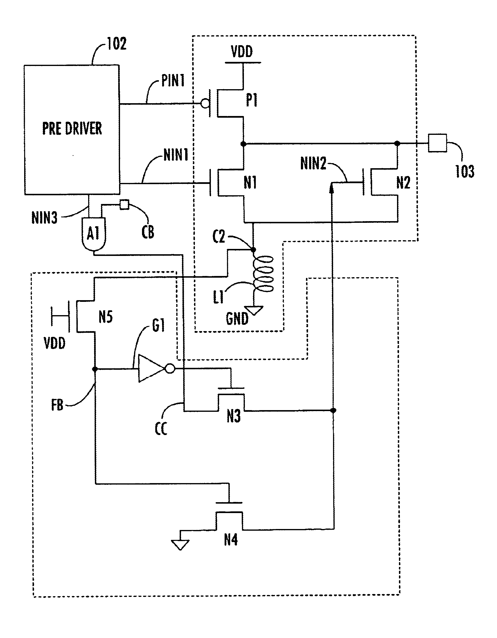
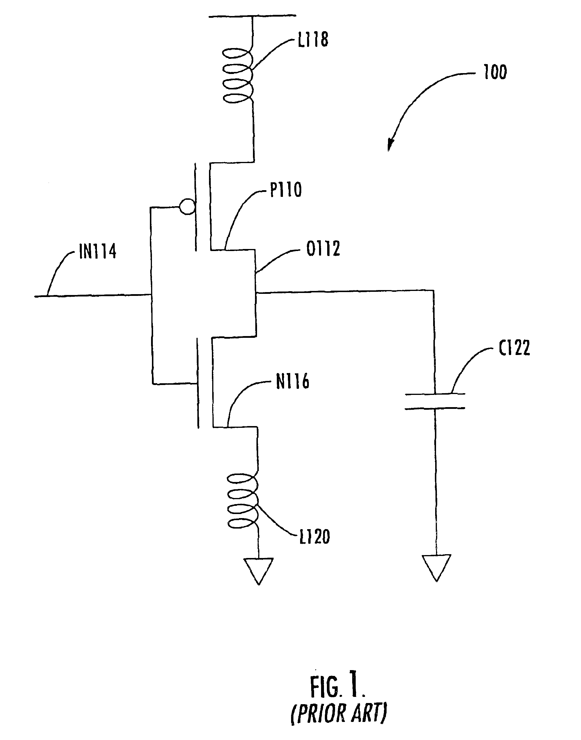
The present invention will now be described more fully hereinafter with reference to the accompanying drawings, in which preferred embodiments of the invention are shown. This invention may, however, be embodied in many different forms and should not be construed as limited to the embodiments set forth herein. Rather, these embodiments are provided so that this disclosure will be thorough and complete, and will fully convey the scope of the invention to those skilled in the art. Like numbers refer to like elements throughout, and prime notation is used to indicate similar elements in alternative embodiments.

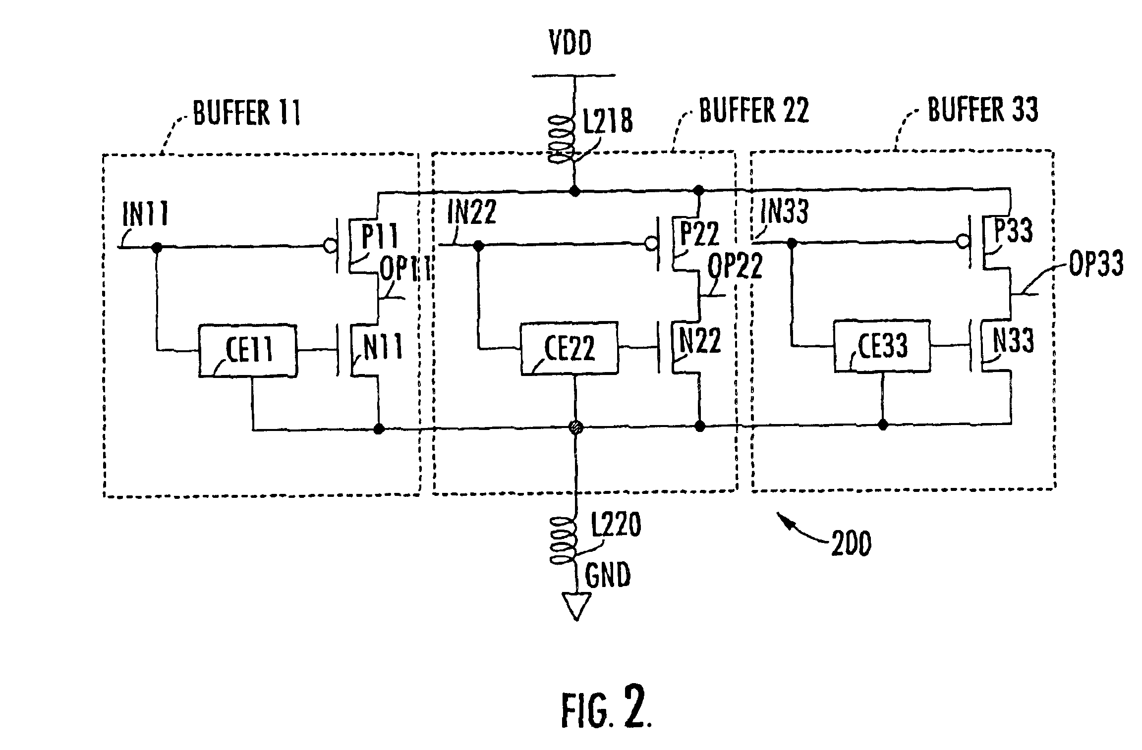
Referring to FIG. 2, three output buffers BUFFER11, BUFFER22, and BUFFER33 in accordance with the invention are connected between common supplies VDD and GND through package inductances on the VDD and GND pins illustratively represented as inductors L218 and L220, respectively. The inputs to the buffers are IN11, IN22, and IN33, respectively, and the outputs are OP11, OP22, and O...


PUM


Abstract

A CMOS output buffer uses feedback from a ground node to reduce ground bounce by utilizing a tolerable ground bounce limit, making it less sensitive to operating conditions and processing parameters. An input to the NMOS device of the output buffer is provided by the output of a control element which receives a first input from a pre-driver and a second input (i.e., the feedback) from the ground node.

Description

FIELD OF THE INVENTIONThe present invention relates to the field of integrated circuits, and, more particularly, to a CMOS buffer.BACKGROUND OF THE INVENTIONIn integrated circuits, output buffers are used for interfacing core logic with external devices. One prominent problem in output buffers is “ground bounce.” More particularly, one basic property of an inductor is that the change of current therethrough produces a voltage across the inductor, which is directly proportional to the rate of change of current through the inductor. This may be represented as:dV=LdI / dT, where dV is the voltage generated, L is the inductance, and dI / dT is the rate of change of the current.Thus, it may be said that the voltage across the inductor bounces. When considered at the ground pin, this is referred to as ground bounce. Ground bounce occurs as a result of parasitic inductance of the integrated circuit and packaging interconnections. Ground bounce occurs when the pull down transistor switches from...

Claims


Application Information

Patent Timeline
Patent Type & Authority Patents(United States)
IPC IPC(8): H03K17/16
CPCH03K17/166
Inventor KAUSHIK, RAJESHNARWAL, RAJESH
Owner STMICROELECTRONICS PVT LTD
Why Eureka
Try Eureka