Methods for manufacturing resistors using a sacrificial layer

Inactive Publication Date: 2005-02-15
TESSERA INC
View PDF46 Cites 125 Cited by
  • Summary
  • Abstract
  • Description
  • Claims
  • Application Information

AI Technical Summary

Benefits of technology

Methods according to the foregoing aspects of the invention provide efficient manufacturing processes for forming resistors and for forming resistor networks incorporating plural resistances. The

Problems solved by technology

The drawback of traditional thick and thin film resistor manufacturing is that both processes tend to have many process steps.
Another drawback to these methods of manufacture is that they are generally not capable of providing resistor networks having multiple different or common values in a single devic

Method used


Image

  • Methods for manufacturing resistors using a sacrificial layer
  • Methods for manufacturing resistors using a sacrificial layer
  • Methods for manufacturing resistors using a sacrificial layer

Examples


Embodiment Construction

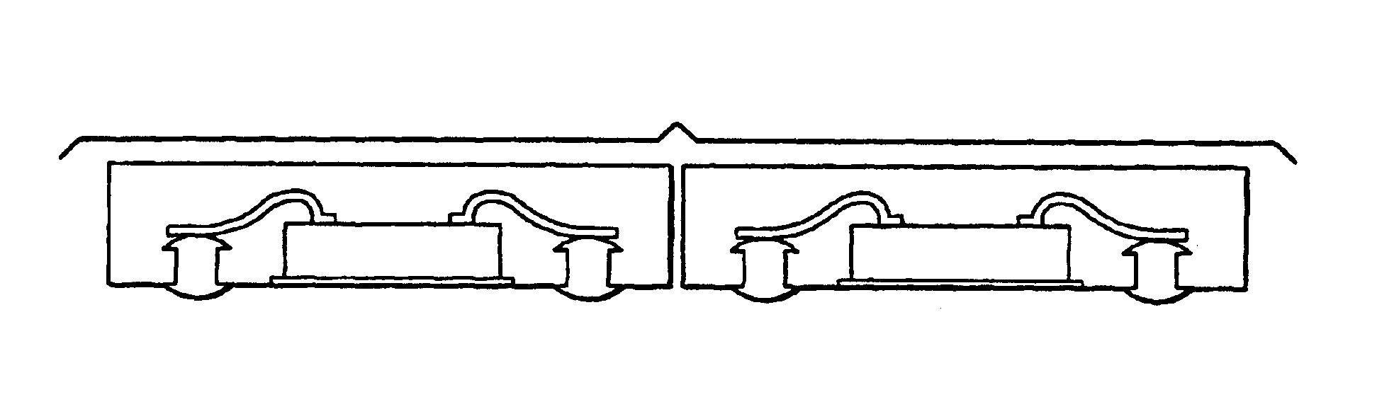
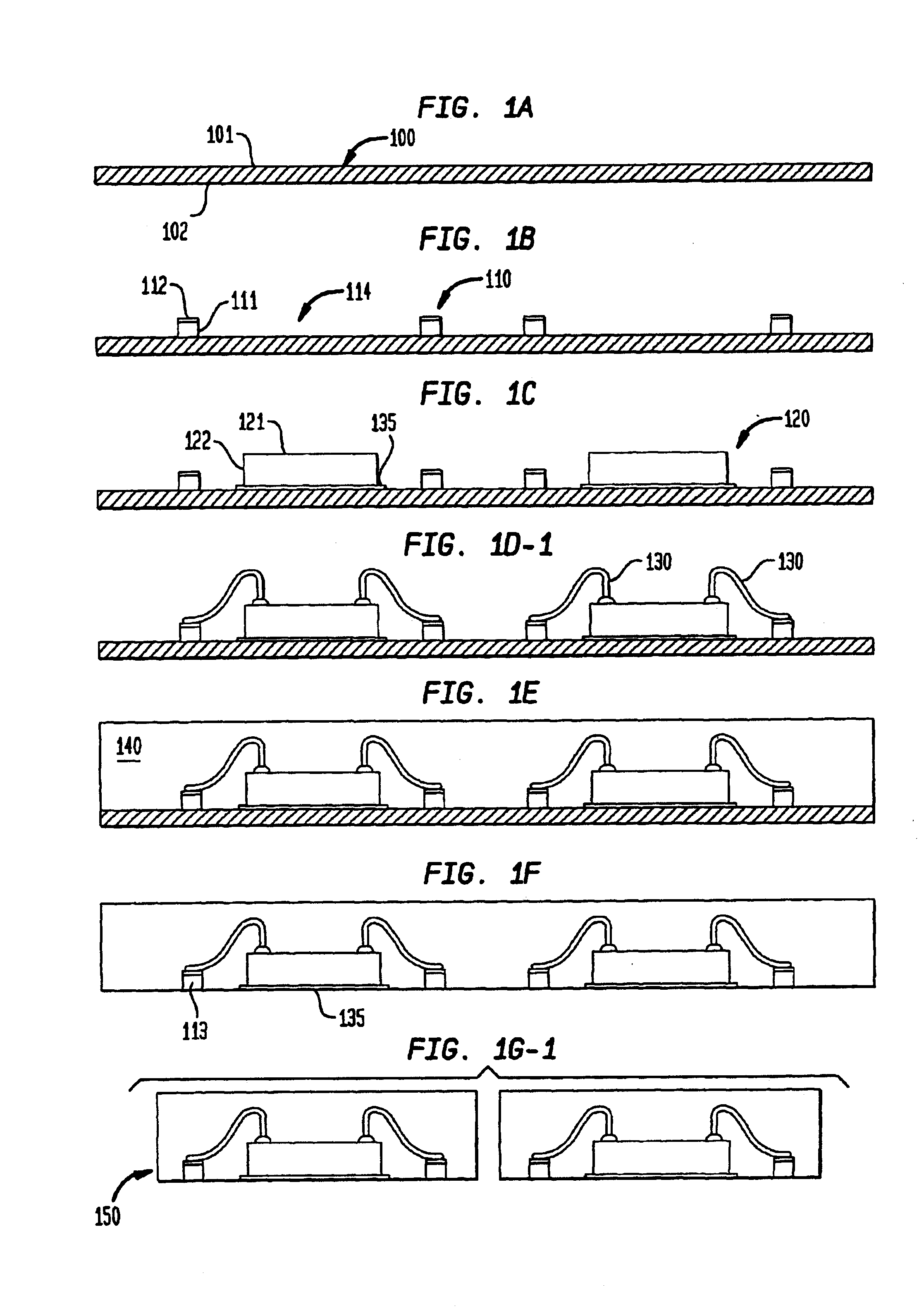
FIGS. 1A-G show a process for manufacturing inexpensive semiconductor chip packages, according to the one aspect of the '671 disclosure. FIG. 1A shows a side view of a sacrificial layer 100 having a first surface 101 and a second surface 102. The sacrificial layer 100 may be comprised of a conductive metallic material, a polymer material or a combination of both a conductive metallic material and a polymer material. Examples of possible sacrificial layer materials include aluminum, copper, steel, iron, bronze, brass, polyimide, polyetherimide, fluropolymer and alloys and combinations thereof. In FIG. 1A, the sacrificial layer is comprised of a sheet of aluminum having an approximate substantially uniform thickness of about 100-200 microns; although, the sacrificial sheet could be thicker or thinner in some embodiments.

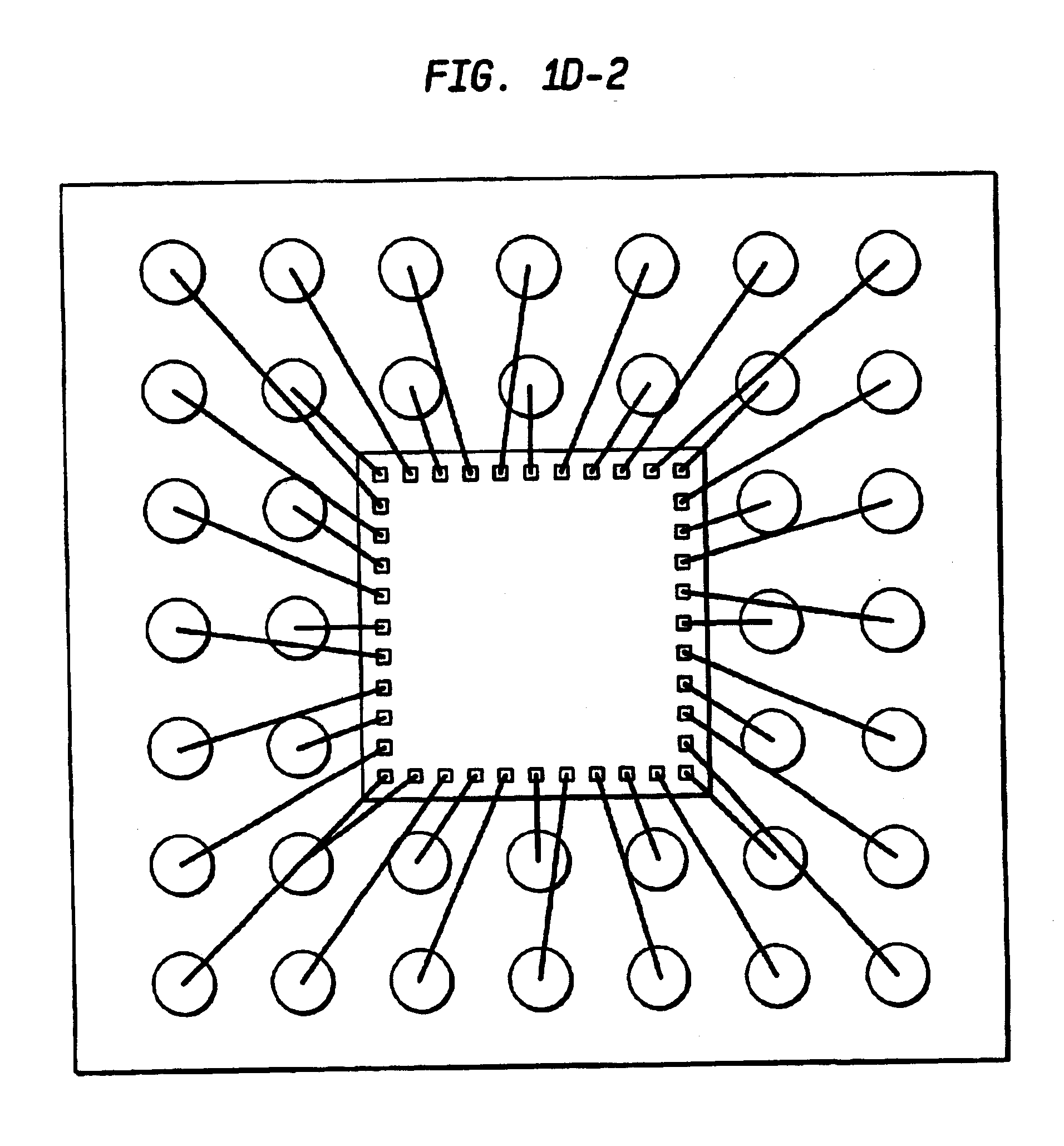
In FIG. 1B, a plurality of pads 110 are selectively formed, typically by an electroplating operation, so that the pads 110 are disposed on and attached to the first su...


PUM

PropertyMeasurementUnit
Electrical conductivityaaaaaaaaaa
Massaaaaaaaaaa
Electrical resistanceaaaaaaaaaa

Abstract

A method of making resistors includes providing a sacrificial layer. Conductive material is then formed over a region of the sacrificial layer. Resistive material is then deposited over the first surface of the sacrificial layer such that the resistive material covers the sacrificial layer and the conductive material. A portion of the sacrificial layer is then removed to expose the conductive material. A method of making resistors includes the steps of providing a sacrificial layer, removing at least a portion of the sacrificial layer from regions of the sacrificial layer so as to create a plurality of cavities within the sacrificial layer, plating said cavities with a conductive material, disposing resistive material over the first surface of the sacrificial layer such that resistive material covers the sacrificial layer and said conductive material, and removing at least a portion of said sacrificial layer to expose the conductive material. In another embodiment, a method of making resistors includes the steps of providing a sacrificial layer having a roughened first surface and a second surface, depositing resistive material over the first surface of the sacrificial layer such that the resistive material covers the first surface of the sacrificial layer, and selectively etching the sacrificial layer to form electrodes.

Description

FIELD OF THE INVENTIONThe present invention generally relates to a resistor network having multiple different or common values in a single device manufactured using a single sacrificial layer.BACKGROUND OF THE INVENTIONResistors are presently fabricated using a number of different methods, depending on the requirements of the circuit in which resistors are to be used. Resistor types such as thin film resistors, thick film resistors, wound wire resistors, molded axial leaded resistors, surface mount resistors and others are known in the art.Thin film resistors are fabricated by first depositing a resistive material, then a conductor material, onto a substrate. A wide variety of substrate materials can be used, but these materials generally contain an oxygen compound to permit adhesion of the resistive film. Materials used for thin film resistors generally must also be capable of providing adhesion to a substrate. The resistor film forms as single points on the substrate in the vicini...

Claims


Application Information

Patent Timeline
IPC IPC(8): D21F1/06D21G9/00H01L21/56H01L21/68H01L23/28H01L21/02H01L23/31H01L21/67H01L21/48H01L25/18
CPCH01L21/4832H01L21/561H01L21/568H01L23/3107H01L23/3121H01L23/3128H01L24/48H01L24/49H01L24/85H01L24/97H01L25/18H01L21/56Y10T29/49099H01L2221/68377H01L2224/05599H01L2224/32245H01L2224/4809H01L2224/48091H01L2224/48095H01L2224/48137H01L2224/48145H01L2224/48227H01L2224/48247H01L2224/48465H01L2224/4847H01L2224/48472H01L2224/48475H01L2224/49171H01L2224/49433H01L2224/73265H01L2224/85001H01L2224/85051H01L2224/85444H01L2224/92H01L2224/92247H01L2224/97H01L2924/01005H01L2924/01006H01L2924/01013H01L2924/01027H01L2924/01028H01L2924/01029H01L2924/0103H01L2924/01047H01L2924/0105H01L2924/01078H01L2924/01079H01L2924/01082H01L2924/014H01L2924/09701H01L2924/19043H01L2924/19107H01L2924/3011H01L2924/00014H01L2924/01024H01L2924/01033H01L2924/01045H01L2924/01076H01L2924/18165Y10T29/49098Y10T29/49101Y10T29/49Y10T29/49002Y10T29/49082H01L2924/181H01L2224/05554H01L2924/12042H01L2924/00H01L2224/85H01L2224/78H01L2224/45099H01L2924/00012H01L2224/45015H01L2924/207
Inventor FJELSTAD, JOSEPH
Owner TESSERA INC
Why Eureka
Try Eureka