Laser processing device and laser processing method

a laser processing device and laser processing technology, applied in the direction of semiconductor lasers, manufacturing tools, active medium materials, etc., can solve the problems of complex apparatus, large size as a whole, and difficulty in enhancing the durability of laser machining apparatus, so as to prevent the generation of blowholes in the welded bead

Inactive Publication Date: 2005-02-15
TOYOTA JIDOSHA KK
View PDF9 Cites 16 Cited by
  • Summary
  • Abstract
  • Description
  • Claims
  • Application Information

AI Technical Summary

Benefits of technology

FIG. 20 is a diagram for illustrating a state where the molten pool is stirred at the rear in the machining direction according to the present invention a

Problems solved by technology

In addition, since it is required to provide the laser machining apparatus with a mechanism for vibrating the condenser lens 3 or a mechanism for repetitively rotating the scanning mirror 4 (its illustration is omitted), the apparatus becomes complicated and large-sized as a whole, and maintenance for maintaining these mechanisms is also required.
Further, the vibration given to the condenser lens and the repetitive rotation of the scanning mirror 4 make it difficult to enhance the durability of the laser machining apparatus.
Further, when cladding buildup is carried out as shown in FIG. 25, since the heat is hard to be released at a center area of the molten portion of the base material, the molten portion tends to grow large.
Especially in the case where the base material is made of copper and the buildup material is made of aluminum, if the base material is diluted and the composition of the buildup material changes, there aris

Method used


Image

  • Laser processing device and laser processing method
  • Laser processing device and laser processing method
  • Laser processing device and laser processing method

Examples


Embodiment Construction

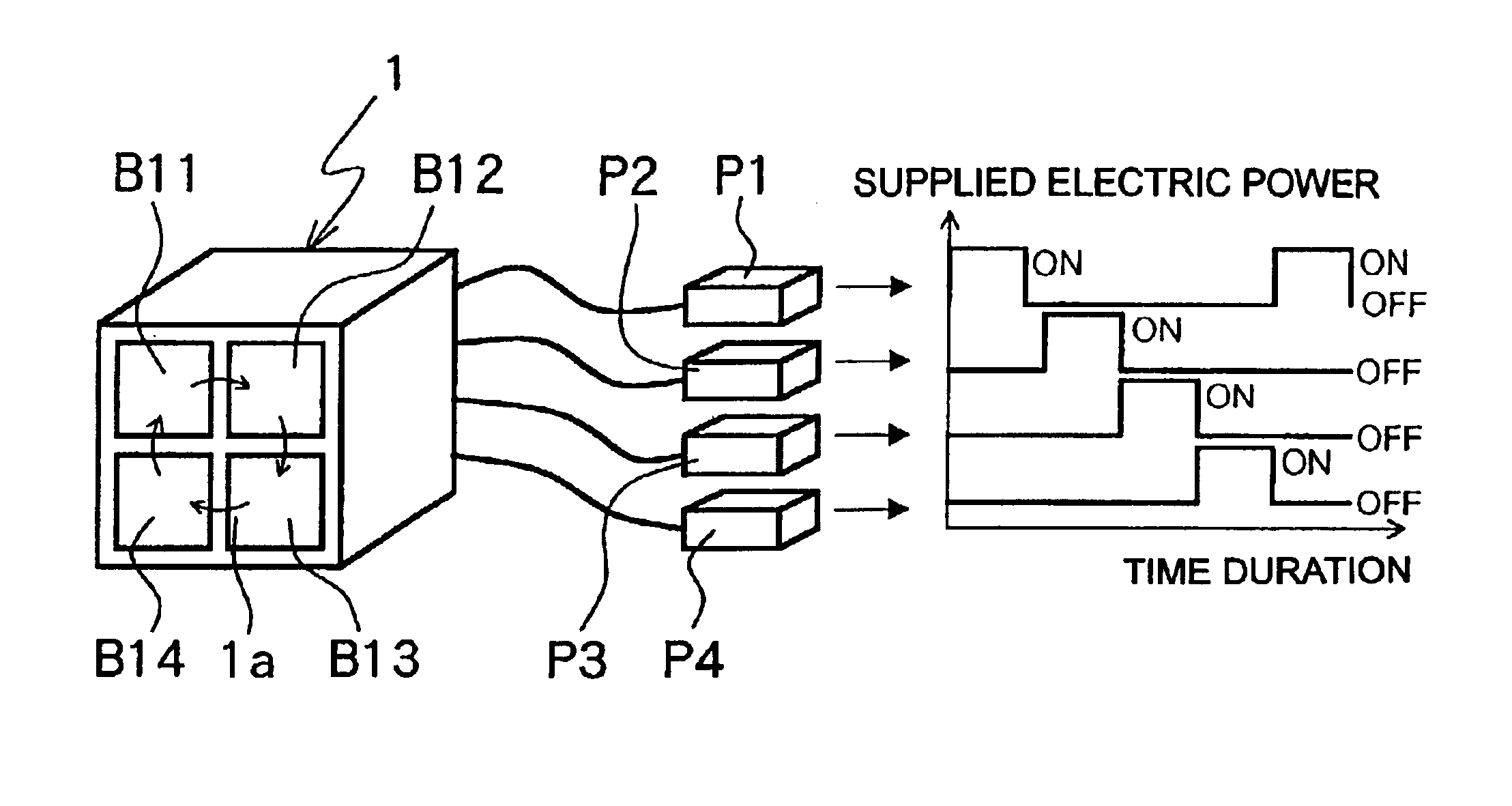
First, an embodiment of the laser machining apparatus of the present invention will be described in detail mainly based on FIG. 1. In the drawings, identical reference numerals and symbols denote the same or corresponding constituent elements.

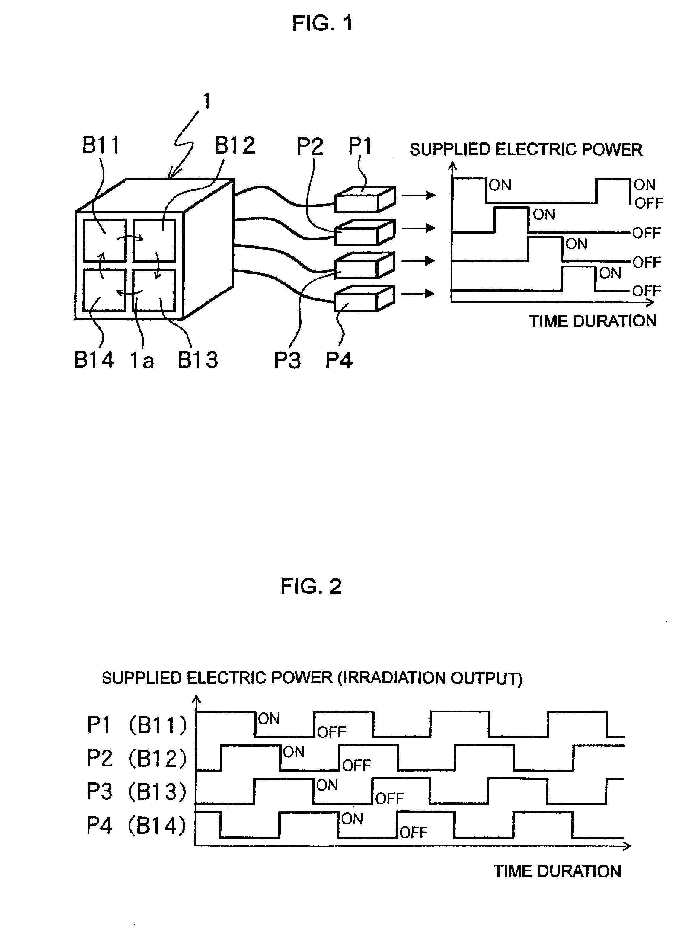
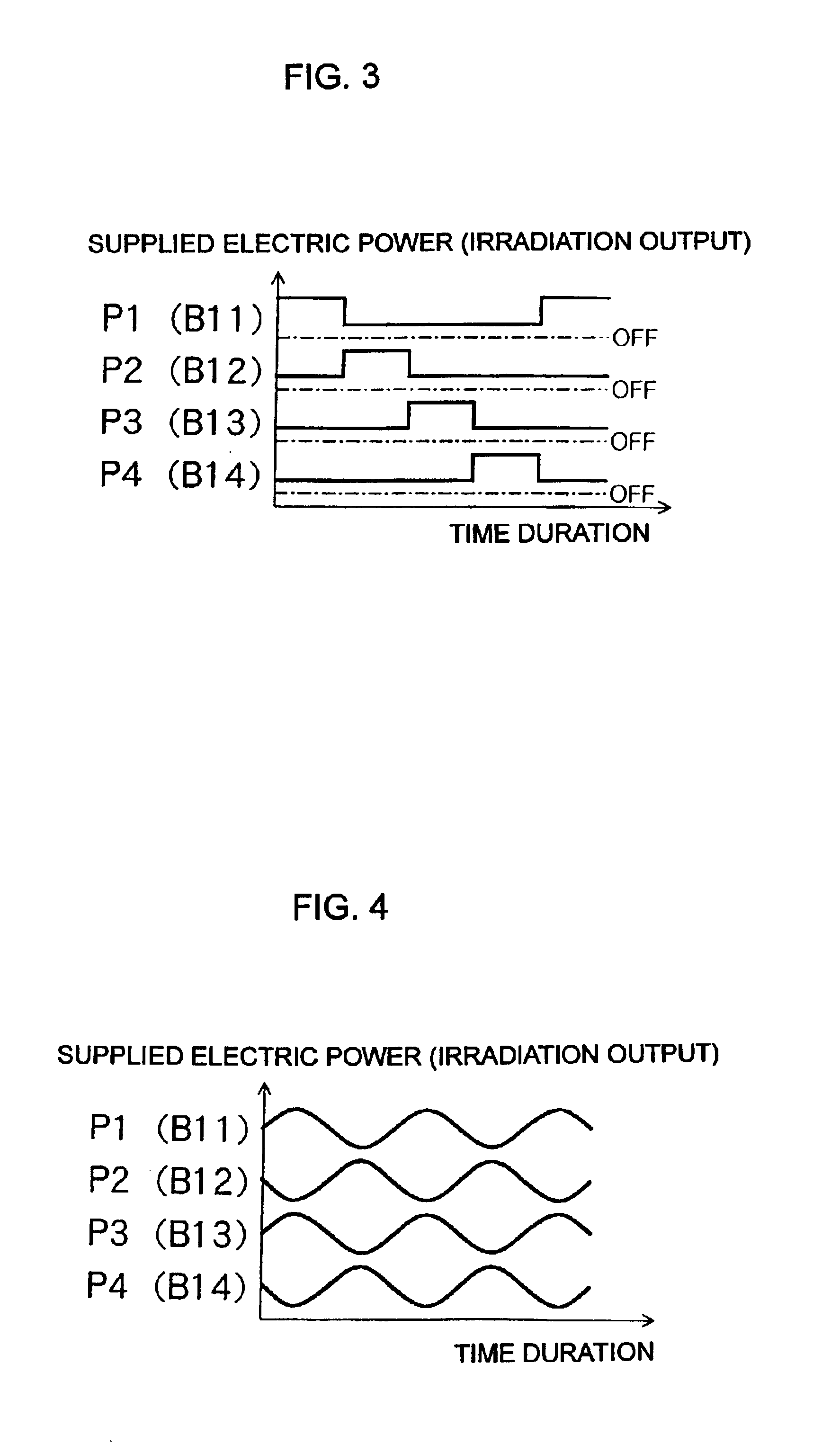
The laser machining apparatus of the present invention generally includes: a semiconductor stack (or also referred to as a semiconductor laser module) 1 including a plurality of semiconductor laser elements (their illustration is omitted); and a controller (although its illustration is omitted, its function will be described later) for controlling emission of the laser beam emitted from each of the semiconductor laser elements. The semiconductor stack 1 is divided into a plurality of blocks B11, B12, B13, B14 in correspondence with the machining-target site Wa of a work piece W. The controller controls the irradiation of the laser beam from each of the blocks B11, B12, B13, B14 to be changeable in terms of time.

Each of the semiconductor laser e...


PUM

PropertyMeasurementUnit
Timeaaaaaaaaaa
Irradiation doseaaaaaaaaaa
Durabilityaaaaaaaaaa

Abstract

The present invention provides a laser machining apparatus in a simple structure which can properly carry out laser machining by irradiating a laser beam easily at a predetermined energy density to a machining-target site in a predetermined range, and in addition, which can be downsized and can be kept with easy maintenance and has enhanced durability.
The apparatus includes: a semiconductor stack 1 comprising a plurality of semiconductor laser elements; and a controller for controlling emission of the laser beam emitted from each of the semiconductor laser elements. The semiconductor stack 1 is divided into a plurality of blocks B11, B12, B13, B14 in correspondence with the machining-target site of a work piece. The controller controls the irradiation of the laser beam from each of the blocks B11, B12, B13, B14 to be changeable in terms of time.

Description

TECHNICAL FIELDThe present invention relates to a laser machining apparatus and a machining method therewith.BACKGROUND ARTMachining such as a heat treatment including cutting, perforation, welding, cladding buildup and quenching has come to be carried out by irradiating a laser beam to a machining-target site of a work piece. In these various kinds of laser machining, in general, a YAG laser beam and a carbon dioxide gas laser have conventionally been employed.When a YAG laser or a carbon dioxide gas laser is employed, in order to obtain an energy density and output corresponding to the laser machining, the emitted laser beam is reduced into a predetermined spot diameter by use of a condenser lens or a condenser reflecting mirror and then is irradiated to the machining-target site. Especially in welding, cladding buildup, quenching and the like where the machining-target site Wa in a predetermined range of a work piece W is machined without turning its state into a gaseous phase, a...

Claims


Application Information

Patent Timeline
IPC IPC(8): B23K26/32B23K26/073B23K26/00B23K26/06B23K26/21B23K26/24B23K26/34
CPCB23K26/0604B23K26/0613B23K26/073B23K26/3206B23K26/328B23K26/3293B23K26/246B23K2203/04B23K26/32B23K26/244B23K2101/35B23K2103/04B23K2103/08B23K2103/16B23K2103/50
Inventor MIKAME, KAZUHISA
Owner TOYOTA JIDOSHA KK
Why Eureka
Try Eureka