Polishing apparatus, semiconductor device manufacturing method using the polishing apparatus, and semiconductor device manufactured by the manufacturing method

a polishing apparatus and polishing technology, applied in the direction of manufacturing tools, semiconductor/solid-state device details, lapping machines, etc., can solve the problems of affecting the manufacturing process of semiconductor devices, affecting the yield of semiconductor devices manufactured by this semiconductor device manufacturing method, and affecting the quality of semiconductor devices. , to achieve the effect of high degree of smoothness, good performance and increased yield of semiconductor devices

Inactive Publication Date: 2005-02-22
NIKON CORP
View PDF18 Cites 27 Cited by
  • Summary
  • Abstract
  • Description
  • Claims
  • Application Information

AI Technical Summary

Benefits of technology

In the polishing apparatus of the present invention, a corrective moment is applied to the polishing member during the polishing of the substrate, so that the polishing member is maintained in a fixed attitude with respect to the surface of the substrate; accordingly, even in cases where the polishing surface protrudes beyond the outer circumference of the substrate, there is no tilting of the polishing member at the outer circumferential edge of the substrate, so that the peripheral portions of the substrate are not caused to slope downward (i.e., are not beveled). As a result, the rate of production of satisfactory substrates is increased, so that manufacturing costs can be reduced.
Furthermore, the semiconductor device manufacturing method of the present invention has a process in which the surface of a substrate is polished using the polishing apparatus. As a result, the yield of semiconductor devices manufactured by this semiconductor device manufacturing method can be increased. Furthermore, the semiconductor device of the present invention is manufactured by the semiconductor device manufacturing method. Since substrates with a high degree of smoothness are used in the semiconductor devices manufactured by the manufacturing method, these devices show good performance, with few problems such as faulty insulation or short-circuiting, etc., of the wiring.

Problems solved by technology

If the precision of polishing performed following such thin film formation is poor, there is a danger that local thinning of the thin films may occur in step areas, and that faulty wiring insulation or short-circuiting, etc., may occur.
Furthermore, in lithographic processes, an out-of-focus state may result if there are numerous indentations and projections in the surface of the wafer, so that it may become impossible to form fine patterns.
Furthermore, the apparatus is arranged so that the contact pressure between the polishing member and the wafer surface is adjusted by means of air pressure that drives the polishing member downward inside the polishing head; however, since such control by means of air pressure has a slow response, the adjustment of the contact pressure cannot be caused to follow the variation in the contact area between the two parts that occurs when the polishing surface protrudes beyond the outer circumference of the wafer.
Accordingly, the polished state of the wafer surface tends not to be uniform.

Method used


Image

  • Polishing apparatus, semiconductor device manufacturing method using the polishing apparatus, and semiconductor device manufactured by the manufacturing method
  • Polishing apparatus, semiconductor device manufacturing method using the polishing apparatus, and semiconductor device manufactured by the manufacturing method
  • Polishing apparatus, semiconductor device manufacturing method using the polishing apparatus, and semiconductor device manufactured by the manufacturing method

Examples


Embodiment Construction

Below, preferred working embodiments of the present invention will be described with reference to the attached figures.

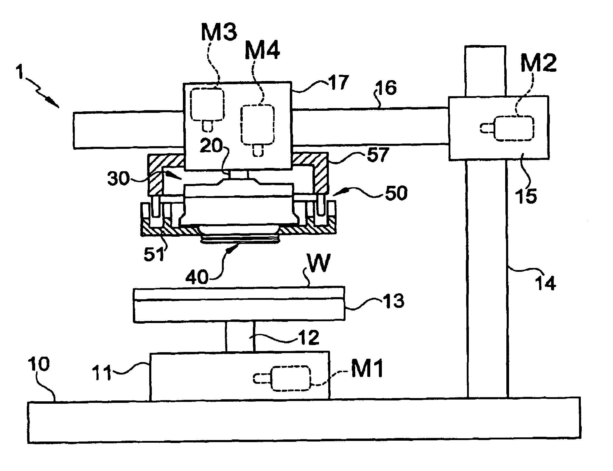
FIG. 1 shows an embodiment in which the polishing apparatus of the present invention is applied to a CMP apparatus (chemical-mechanical polishing apparatus). In this CMP apparatus 1, a table supporting part 11 is installed on the upper surface of a base stand 10, and a shaft 12 is supported on this table supporting part 11 so that the shaft 12 extends vertically and is free to rotate. A rotating table 13 is installed in a horizontal attitude on the upper end of this shaft 12. A wafer W is held by vacuum suction on the upper surface side of the rotating table 13 as a substrate which constitutes the polished member. This rotating table 13 is caused to rotate in the horizontal plane by driving the shaft 12 by means of an electric motor M1 contained in the table supporting part 11.

A supporting column 14 is installed so that it extends vertically to one side of the table...


PUM

PropertyMeasurementUnit
contact pressureaaaaaaaaaa
electromagnetic forceaaaaaaaaaa
magnetic fieldaaaaaaaaaa

Abstract

The present invention provides a polishing apparatus with a construction which makes it possible to prevent the peripheral portions of a substrate from sloping downward as a result of the polishing member tilting at the peripheral portions of the substrate during the polishing of the substrate, and which makes it possible to adjust the contact pressure quickly in accordance with changes in the contact area between the polishing surface and the substrate surface.

Description

BACKGROUND OF THE INVENTION1. Field of the InventionThe present invention relates to a polishing apparatus which polishes and smooths the surface of a substrate such as a wafer, etc., used in semiconductor devices, a semiconductor device manufacturing method using this apparatus, and a semiconductor device manufactured by this manufacturing method.2. Description of the Related ArtIn recent years, as IC's have become finer and more complex, and as the number of layers of multi-layer wiring has increased, the steps on IC surfaces have become increasingly larger, and the precision of polishing wafer surfaces that is performed following the formation of respective thin films has become more important. If the precision of polishing performed following such thin film formation is poor, there is a danger that local thinning of the thin films may occur in step areas, and that faulty wiring insulation or short-circuiting, etc., may occur. Furthermore, in lithographic processes, an out-of-foc...

Claims


Application Information

Patent Timeline
Patent Type & Authority Patents(United States)
IPC IPC(8): B24B37/04B24B41/00B24B41/04B24B49/10B24B37/005H01L21/304
CPCB24B37/30B24B49/10B24B41/068B24B41/042H01L21/304
Inventor HAYASHI, YUTAKAUDA, YUTAKA
Owner NIKON CORP
Why Eureka
Try Eureka