Method for fabricating semiconductor packages, and leadframe assemblies for the fabrication thereof

a technology of leadframe and semiconductor package, which is applied in the direction of semiconductor devices, basic electric elements, electrical equipment, etc., can solve the problems of large configuration, high tooling cost for manufacturing a new package, and designer often compromises

Inactive Publication Date: 2005-02-22
STATS CHIPPAC LTD
View PDF2 Cites 37 Cited by
  • Summary
  • Abstract
  • Description
  • Claims
  • Application Information

AI Technical Summary

Problems solved by technology

The CSP therefore saves considerable space over earlier, larger configurations.
Thus, the tooling cost for manufacturing a new package can be high.
Therefore, rather than creating a package that is optimized specifically for a given IC size and input / output (“I / O”) configuration, a designer often compromises by selecting an already available package instead.
In such a case, unfortunately, the resulting package is optimized for neither density nor material cost.
However, there are still significant disadvantages with both punch singulation and saw singulation.
For example, punch singulation wastes leadframe space (circuit area), can suffer from debris damage, and requires molds and singulation dies that are individually sized for each leadframe body size.
This causes increased tooling investments or suboptimized design compromises.
Saw singulation processes can form voids, can suffer strip warpage from differences in the thermal expansion of the material layers used, and can be impaired by materials that outgas.
Solutions to these problems have been long sought but prior developments have not taught or suggested any solutions and, thus, solutions to these problems have long eluded those skilled in the art.

Method used


Image

  • Method for fabricating semiconductor packages, and leadframe assemblies for the fabrication thereof
  • Method for fabricating semiconductor packages, and leadframe assemblies for the fabrication thereof
  • Method for fabricating semiconductor packages, and leadframe assemblies for the fabrication thereof

Examples


Embodiment Construction

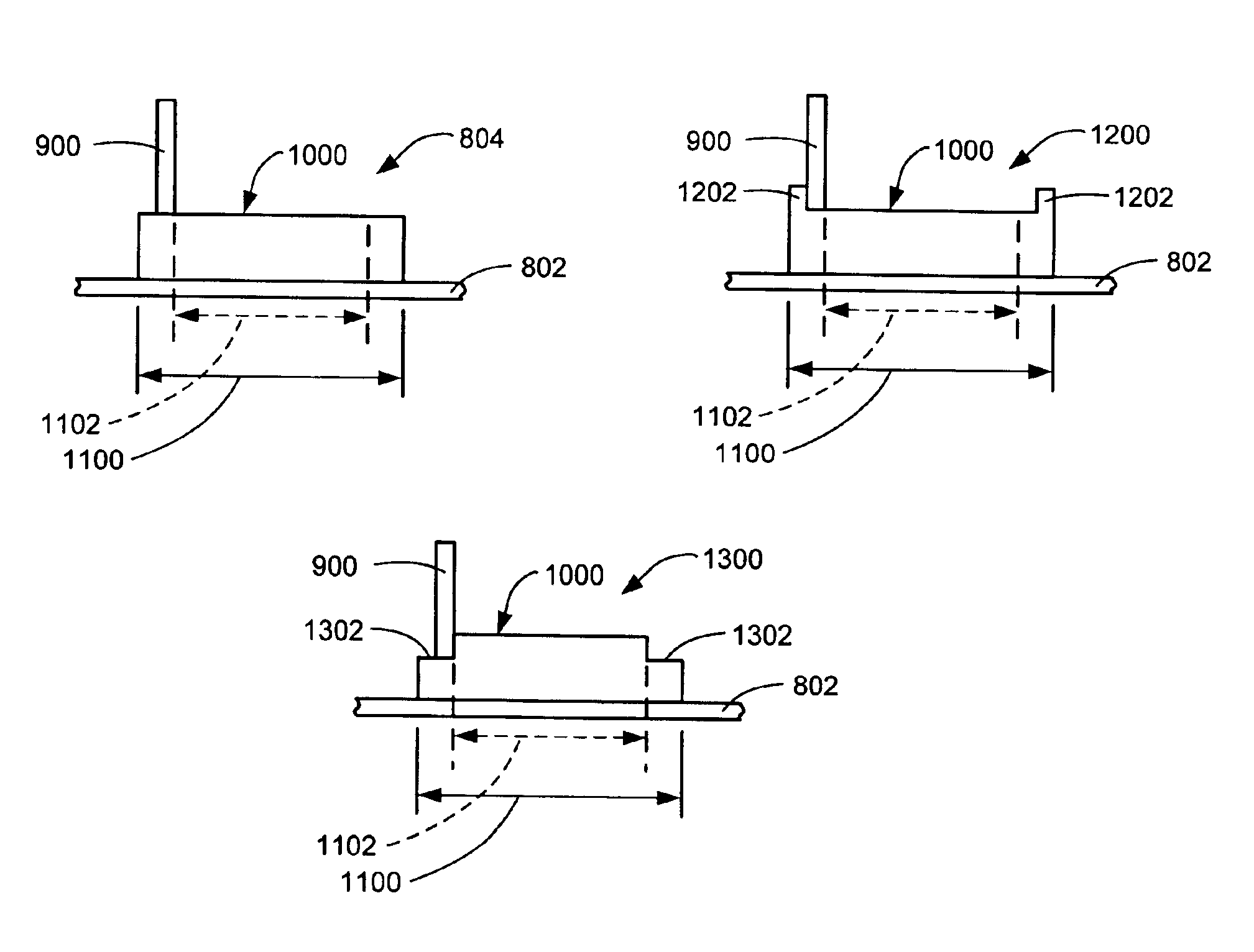
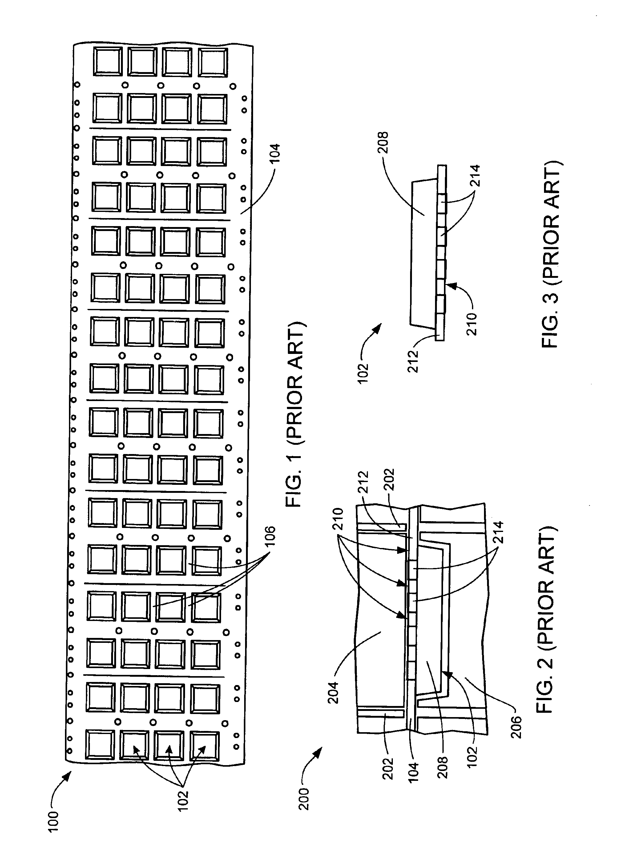
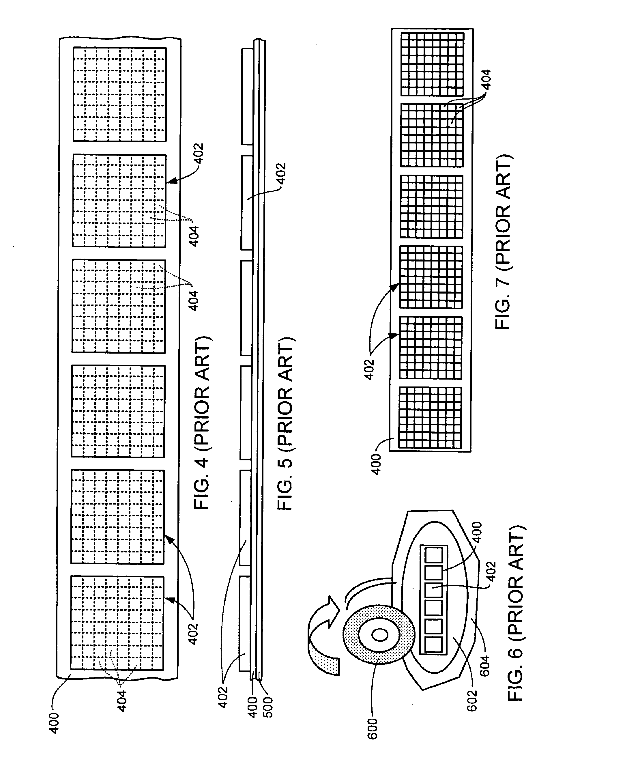
In the following description, numerous specific details are given to provide a thorough understanding of the invention. However, it will be apparent that the invention may be practiced without these specific details. In order to avoid obscuring the present invention, some well-known configurations and process steps are not disclosed in detail. Likewise, the drawings showing embodiments of the invention are semi-diagrammatic and not to scale and, particularly, some of the dimensions are for the clarity of presentation and are shown exaggerated in the drawing FIGs. Also, where multiple embodiments are disclosed and described having some features in common, for clarity and ease of illustration and description thereof like features one to another will ordinarily be described with like reference numerals.

The term “horizontal” as used herein is defined as a plane parallel to the conventional major plane or surface of the semiconductor package, regardless of its orientation. The term “vert...


PUM


Abstract

A method for fabricating semiconductor packages provides a leadframe for packages that are to be singulated with respective predetermined package body sizes. Individual mold caps are formed on the leadframe with mold cap dimensions that are larger than the respective predetermined package body sizes. The mold caps and leadframe are sawed to singulate packages therefrom. The sawing reduces the dimensions of the mold caps to the respective predetermined package body sizes.

Description

TECHNICAL FIELDThe present invention relates generally to semiconductor devices, and more particularly to a method for fabricating semiconductor packages and to leadframe assemblies utilized in the fabrication thereof.BACKGROUND ARTContinuing progress in integrated circuit (“IC”) technology continues to lead to higher and higher levels of circuit integration. This is a result of the computer industry's relentless drive toward higher performance, lower cost, increased miniaturization of components, and greater packaging density of integrated circuits. As new generations of integrated circuit products are released, the functionality of those products increases while the number of components used to fabricate them decreases.Semiconductor devices are constructed from a silicon or gallium arsenide wafer through a process that comprises a number of deposition, masking, diffusion, etching, and implanting steps. Usually, many individual devices are constructed on the same wafer. When the de...

Claims


Application Information

Patent Timeline
Patent Type & Authority Patents(United States)
IPC IPC(8): H01L21/56H01L21/02H01L21/48
CPCH01L21/4842H01L21/565H01L2924/0002H01L2924/00
Inventor HAN, BYUNG JOONAHN, BYUNG HOON
Owner STATS CHIPPAC LTD
Why Eureka
Try Eureka