
Semiconductor device including a capacitance

a technology of capacitance and semiconductor devices, which is applied in semiconductor devices, diodes, electrical equipment, etc., can solve the problems of series resistance increasing and the q-value of insulated gate type capacitance generally small, and achieve the effect of reducing the resistance value of the gate electrod

Inactive Publication Date: 2005-02-22
TESSERA ADVANCED TECH
View PDF12 Cites 5 Cited by
  • Summary
  • Abstract
  • Description
  • Claims
  • Application Information

AI Technical Summary

Benefits of technology

[0033]A capacitance having a great Q-value is used for at least one of the fixed capacitance and the variable capacitance. Consequently, it is possible to enhance the Q-value of a composite capacitance of the fixed capacitance and the variable capacitance.
[0035]The junction capacitance is formed on the SOI substrate. Consequently, it is possible to obtain the junction capacitance which is less influenced by the parasitic capacitance.
[0039]The junction capacitance is formed on the SOI substrate. Consequently, it is possible to obtain the junction capacitance which is less influenced by the parasitic capacitance.
[0043]The electrical connection to the external wiring can be carried out through the first and second contact pad portions. Consequently, it is possible to reduce a resistance value attendant on the gate electrode for a capacitance.
[0045]The gate electrode for a capacitance is constituted by a plurality of partial gate portions. Consequently, a length of each partial gate portion is defined as a gate width. Thus, it is possible to reduce the resistance value of the gate electrode.

Problems solved by technology

Therefore, there has been a problem in that a series resistance is increased.
In addition, there has been a problem in that an insulated gate type capacitance generally has a small Q-value.

Method used


Image

  • Semiconductor device including a capacitance
  • Semiconductor device including a capacitance
  • Semiconductor device including a capacitance

Examples


first embodiment

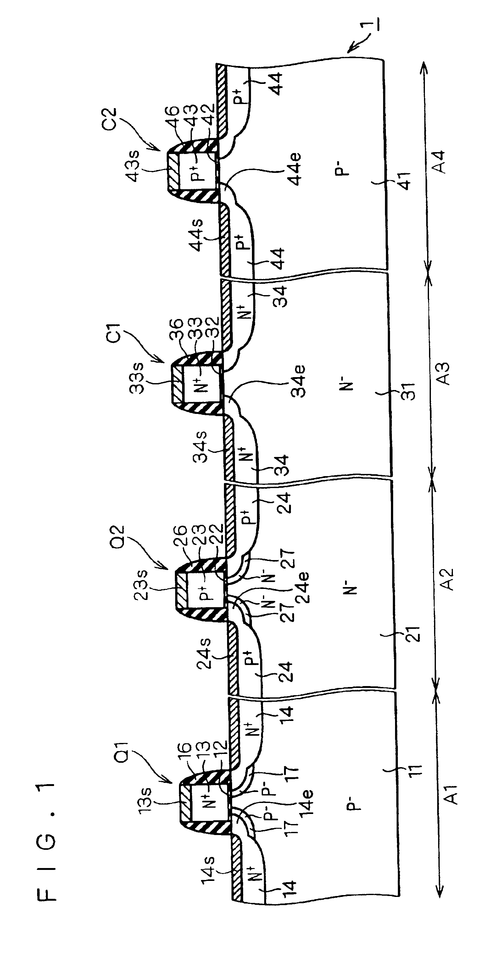
[0087]FIG. 1 is a sectional view showing a structure of a semiconductor device having a MOS transistor and a variable capacitance according to the present invention.

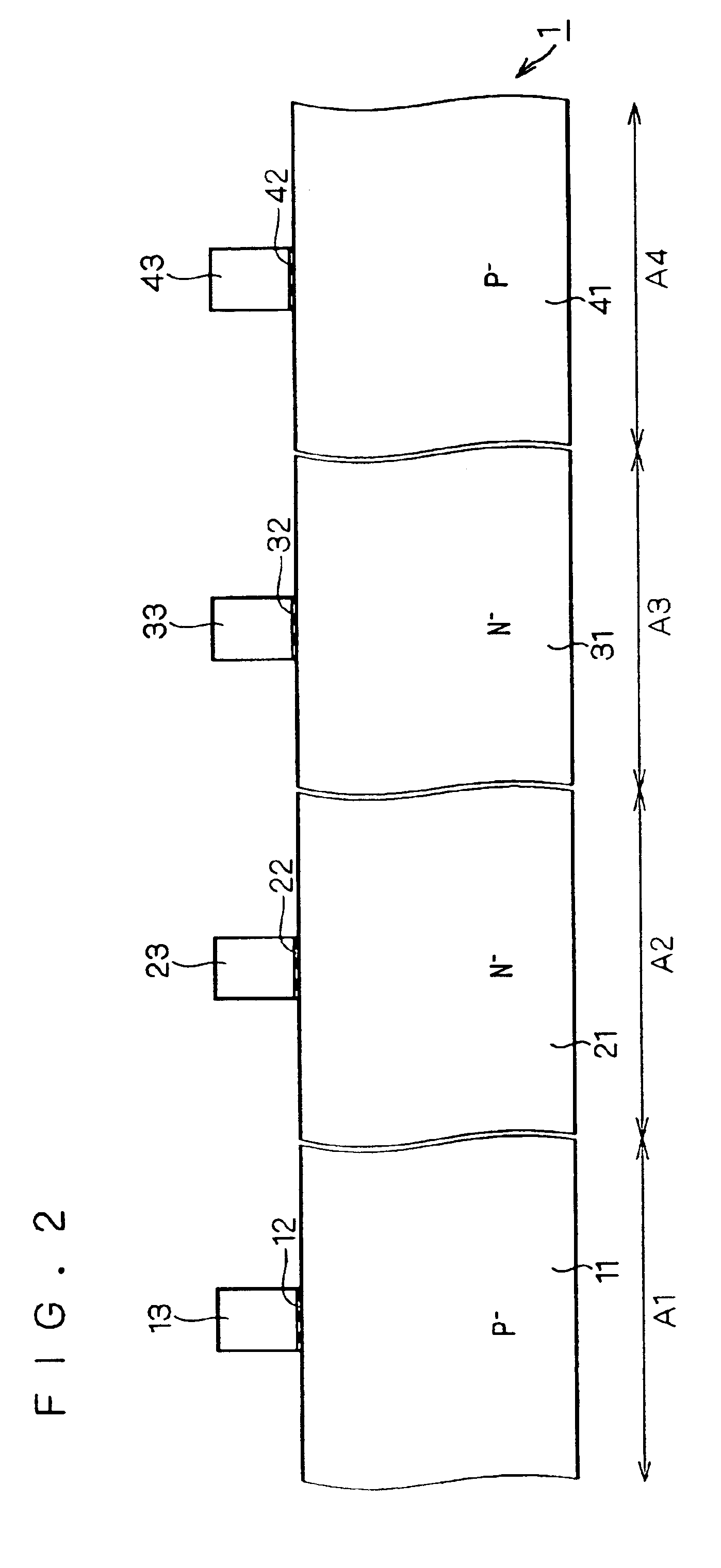
[0088]As shown in FIG. 1, an NMOS transistor Q1, a PMOS transistor Q2, an N-type variable capacitance C1 and a P-type variable capacitance C2 are formed in an NMOS formation region A1, a PMOS formation region A2, an N-type variable capacitance formation region A3 and a P-type variable capacitance formation region A4, respectively. Each of the formation regions A1 to A4 is isolated by an isolating film (not shown) or the like. Moreover, well regions 11, 21, 31 and 41 to be body regions are formed in the formation regions A1, A2, A3 and A4, respectively.

[0089]In the NMOS formation region A1, a gate oxide film 12 is selectively formed on a surface of the P well region 11 and an N+-type gate electrode 13 is formed on the gate oxide film 12. N+ source-drain regions 14 and 14 are formed to interpose therebetween a channel regi...

second embodiment

[0121]FIG. 8 is a sectional view showing a structure of a semiconductor device having a MOS transistor and a variable capacitance according to the present invention.

[0122]As shown in FIG. 8, a buried oxide film 4 is formed on a support substrate 3, and an SOI layer 5 formed on the buried oxide film 4 is isolated into an NMOS formation region A1, a PMOS formation region A2, an N-type variable capacitance formation region A3 and a P-type variable capacitance formation region A4 through an isolating film (not shown) or the like.

[0123]An NMOS transistor Q1, a PMOS transistor Q2, an N-type variable capacitance C1 and a P-type variable capacitance C2 which have the same structures as those of the first embodiment are formed in the NMOS formation region A1, the PMOS formation region A2, the N-type variable capacitance formation region A3 and the P-type variable capacitance formation region A4, respectively.

[0124]In the semiconductor device according to the second embodiment, thus, the MOS ...

third embodiment

[0129]FIG. 11 is a sectional view showing a structure of a semiconductor device having a MOS transistor and a variable capacitance according to the present invention.

[0130]As shown in FIG. 11, variable capacitances C3 and C4 of an inversion type are provided in place of the variable capacitances C1 and C2 of an accumulation type. More specifically, the structure according to the third embodiment is different from the structure according to the first embodiment shown in FIG. 1 in that a P well region 30 is provided in place of the N well region 31 and an N well region 40 is provided in place of the P well region 41.

[0131]More specifically, the N-type (N+ gate / P− body / N+S / D type) variable capacitance C3 and the P-type (P+ gate / N− body / P+S / D type) variable capacitance C4 have structures equivalent to the structures of the NMOS transistor and the PMOS transistor, and are different from the NMOS transistor Q1 and the PMOS transistor Q2 in that pocket regions corresponding to the pocket r...


PUM


Abstract

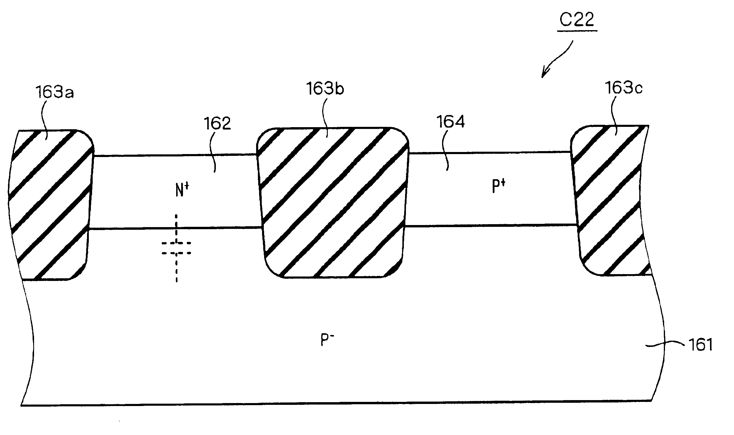
It is an object to obtain a semiconductor device including a capacitance having a great Q-value. In an SOI substrate comprising a support substrate (165), a buried oxide film (166) and an SOI layer (171), an isolating oxide film 167 (167a to 167c) is selectively formed in an upper layer portion of the SOI layer (171) with a part of the SOI layer (171) remaining as a P− well region (169). Consequently, an isolation (partial isolation) structure is obtained. An N+ diffusion region (168) is formed in the SOI layer (171) between the isolating oxide films (167a) and (167b) and a P+ diffusion region (170) is formed in the SOI layer (171) between the isolating oxide films (167b) and (167c). Consequently, there is obtained a junction type variable capacitance (C23) having a PN junction surface of the P− well region (169) provided under the isolating oxide film (167b) and the N+ diffusion region (168).

Description

BACKGROUND OF THE INVENTION[0002]1. Field of the Invention[0003]The present invention relates to a semiconductor device having an insulated gate type transistor and an insulated gate type capacitance and a method of manufacturing the semiconductor device.[0004]2. Description of the Background Art[0005]In a transistor having a gate length of a subquarter micron or less, a pocket injecting process for forming a pocket region is executed in order to suppress a short channel effect. The pocket injection is also referred to as NUDC (Non Uniformly Doped Channel).[0006]FIG. 52 is a sectional view showing the pocket injecting process. As shown in FIG. 52, in the formation of a CMOS transistor, an NMOS formation region A11 and a PMOS formation region A12 are isolated from each other through an isolating film 102 provided in an upper layer portion of a semiconductor substrate 101.[0007]In the NMOS formation region A11, a gate oxide film 112 and a gate electrode 113 are formed on a surface of ...

Claims


Application Information

Patent Timeline
Patent Type & Authority Patents(United States)
IPC IPC(8): H01L29/66H01L29/94H01L27/06H01L27/08H01L21/822H01L27/04H01L21/8234H01L21/8238H01L27/092H01L29/786
CPCH01L21/84H01L27/0629H01L27/0808H01L29/94H01L27/1203H01L29/66181H01L29/66545H01L27/0811
Inventor MAEDA, SHIGENOBUIPPOSHI, TAKASHIHIRANO, YUUICHI
Owner TESSERA ADVANCED TECH
Learn More