Method for examining structures on a semiconductor substrate

a technology of semiconductor substrates and structures, applied in the direction of material analysis, instruments, electrical equipment, etc., can solve the problems of inability to reconstruct three-dimensional structures more deeply, the resolution limit of the acoustic microscope is near, and the inability to operate close to the resolution limit of the microscope, etc., to achieve the effect of improving the resolution, short exposure time, and reducing the damag

Inactive Publication Date: 2005-02-22
SCHNEIDER GERD DR +1
View PDF9 Cites 26 Cited by
  • Summary
  • Abstract
  • Description
  • Claims
  • Application Information

AI Technical Summary

Benefits of technology

The technical effect of this patent is that it describes how to examine structures on semiconductor devices without damaging them or having to remove them from their original position. This allows for quicker observation times, higher accuracy, and continuous monitoring during operational use. Compared to traditional microscopes, these methods provide much more detail about what's happening inside those structures.

Problems solved by technology

The technical problem addressed in this patent text relates to the difficulty of inspecting semiconductor devices containing complex structures, such as conductor paths, using traditional techniques like visual inspection or electron microscopy. Existing methods like X-ray microscopy and surface-sensitive methods like atomic force microscopy (AFM) have limitations in providing high-resolution images. Other issues include the need for improved understanding failomegmatism caused by uncertaintedly affecting the decision making use of passivation levels and the absence of effective removal of films.

Method used


Image

  • Method for examining structures on a semiconductor substrate
  • Method for examining structures on a semiconductor substrate
  • Method for examining structures on a semiconductor substrate

Examples


Embodiment Construction

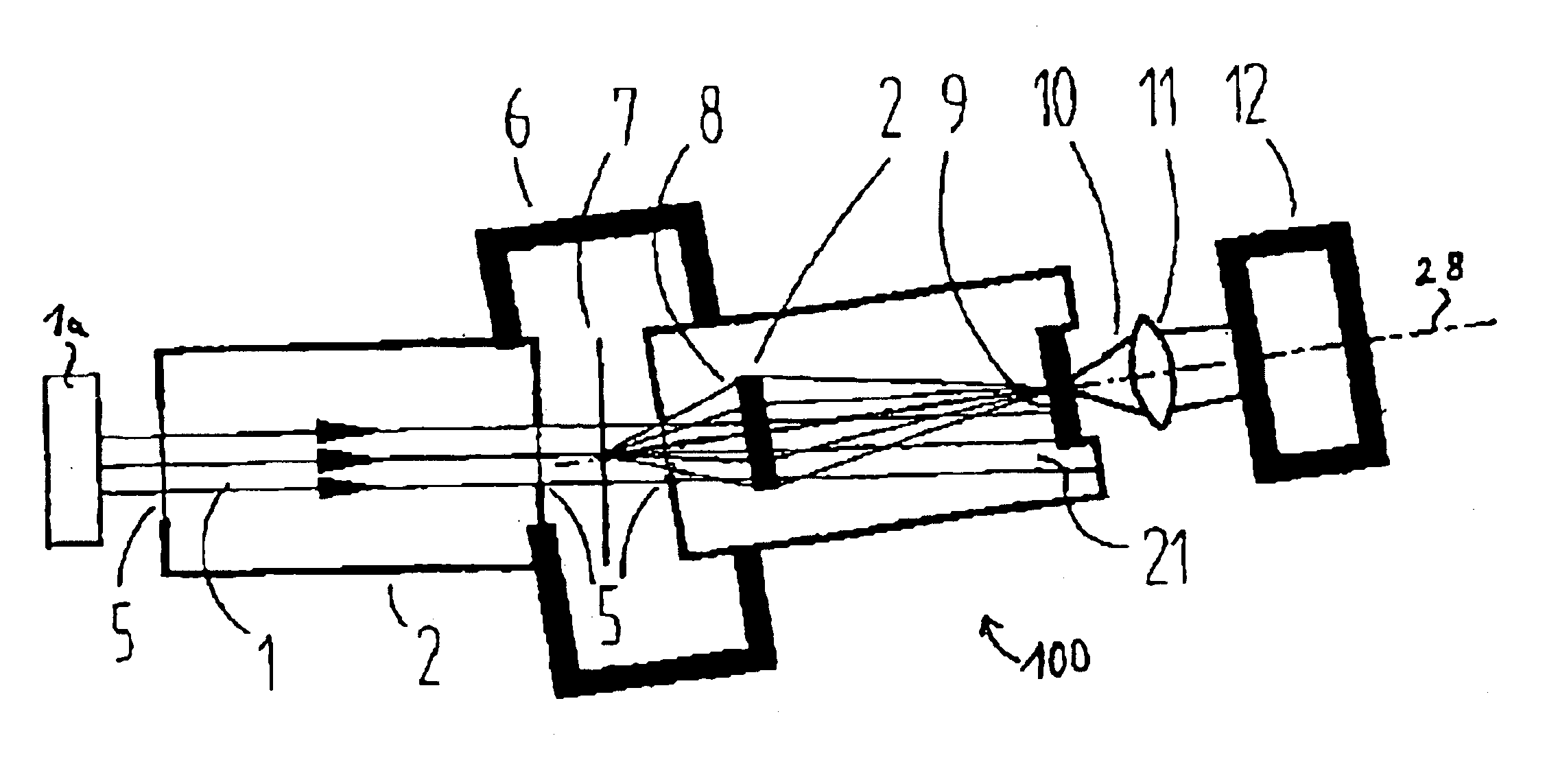
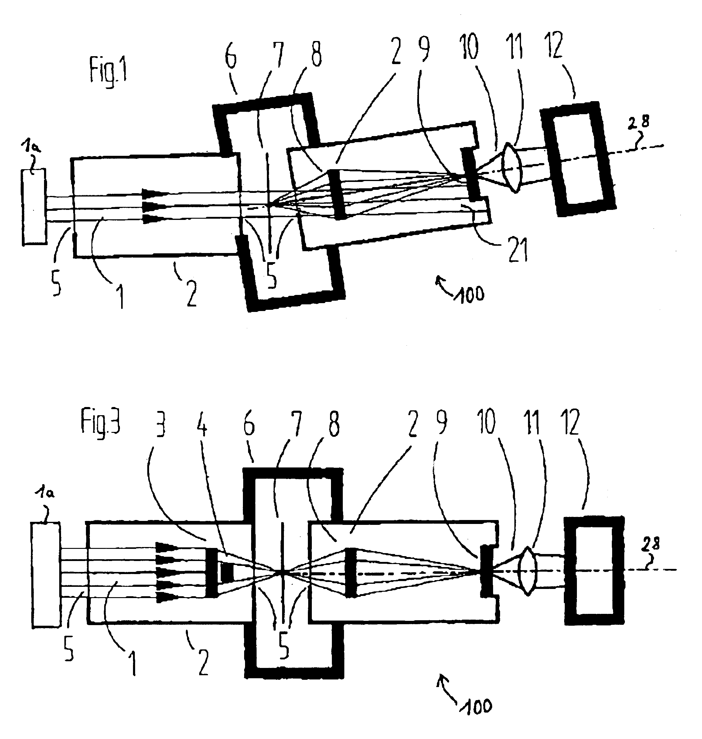
FIG. 1 schematically shows an X-ray microscope 100 that operates without a condenser. This means that X-radiation 1 generated by an X-ray source 1 a (e.g. an electron storage ring) impinges upon specimen 7 under examination without further focusing. Specimen 7 is a semiconductor substrate which has micromechanical or electronic structures that are to be examined. As shown in FIG. 1, X-radiation 1 passes through a vacuum chamber 2, sealed vacuum-tight with X-ray windows 5, in which vacuum prevents absorption of the X-radiation. Radiation 1, propagating along a straight line, illuminates specimen 7 which is located, in air, in a specimen chamber 6.

An imaging objective 8 images a region of specimen 7 onto an X-ray converter 9, which converts the X-radiation into an optical radiation 10 that usually lies in the visible wavelength region. Optical radiation 10 is imaged through a lens 11 by a camera 12. X-ray converter 9, lens 11, and camera 12 thus form a detector device for the X-radiat...


PUM


Abstract

The invention is based on a method for examining structures on a semiconductor substrate. The structures are imaged with X-radiation in an X-ray microscope. The wavelength of the X-radiation is established as a function of the thickness of the semiconductor substrate in such a way that both a suitable transmission of the X-radiation through the semiconductor substrate and a high-contrast image are obtained. As a result, the structures can be observed continuously with short exposure times, high resolution and even while they are in operation.

Description


Claims


Application Information

Patent Timeline
Owner SCHNEIDER GERD DR
Why Eureka
Try Eureka