Semiconductor device with stacked-semiconductor chips and support plate

a technology of semiconductor devices and support plates, which is applied in the direction of semiconductor devices, semiconductor/solid-state device details, electrical apparatus, etc., can solve the problems of difficult to properly bond an end of the wire, the wirebonding machine cannot be used for the wirebonding operation, and the prior art has the following problems, so as to reduce the overall thickness of the semiconductor device

Inactive Publication Date: 2005-03-01
ROHM CO LTD
View PDF30 Cites 30 Cited by
  • Summary
  • Abstract
  • Description
  • Claims
  • Application Information

AI Technical Summary

Benefits of technology

According to the above arrangement, it becomes possible to decrease the height difference between each of the electrode on the semiconductor chips and corresponding one of the terminal portions to be connected via the wire, even if there is a large height difference between the uppermost electrodes and the lowermost electrodes in the stack of plural semiconductor chips. Therefore, it becomes possible to properly connect all of the electrodes on each of the semiconductor chips to respective terminal portions by means of wirebonding, within the vertical moving range of the capillary of the wirebonding machine. Further, it becomes possible to press the capillary of the wirebonding machine to each of the electrodes and terminal portions at a smaller angle of tilt so that the wire can be tightly pressed against the surface of the electrode or terminal portion.
According to the above arrangement, it becomes possible to keep the height difference between the electrodes on each of the semiconductor chips and the terminal portions on the plate type supporting member corresponding not greater than a predetermined distance. Thus, connection can be properly made between the electrodes and the terminal portions by means of wirebonding. In addition, it becomes possible to further reduce the overall thickness of the semiconductor device. It should be noted however, that the electrical connection between the terminal portions on the supporting member and the electrodes on the semiconductor chips may not necessarily be by means of wirebonding. Alternatively for example, one or both of the electrodes and the terminal portions may be formed with bumps for press-fit bonding.

Problems solved by technology

However, the prior art has following problems.
Sometimes, however, the height difference Ha is greater than the upper limit (i.e. greater than the baseline height added with +300 μm), making impossible to use the wirebonding machine for the wirebonding operation.
As a result, according to the prior art, it is difficult to properly bond an end of the wire 93 to the electrodes 94a-94c or the terminal 92, and there is a significant risk of causing a faulty connection at the location where the wire is bonded.

Method used


Image

  • Semiconductor device with stacked-semiconductor chips and support plate
  • Semiconductor device with stacked-semiconductor chips and support plate
  • Semiconductor device with stacked-semiconductor chips and support plate

Examples


Embodiment Construction

Preferred embodiments of the present invention will be described in specific details, referring to the accompanying drawings.

Referring first to FIGS. 1 through 10, the first aspect of the present invention will be described.

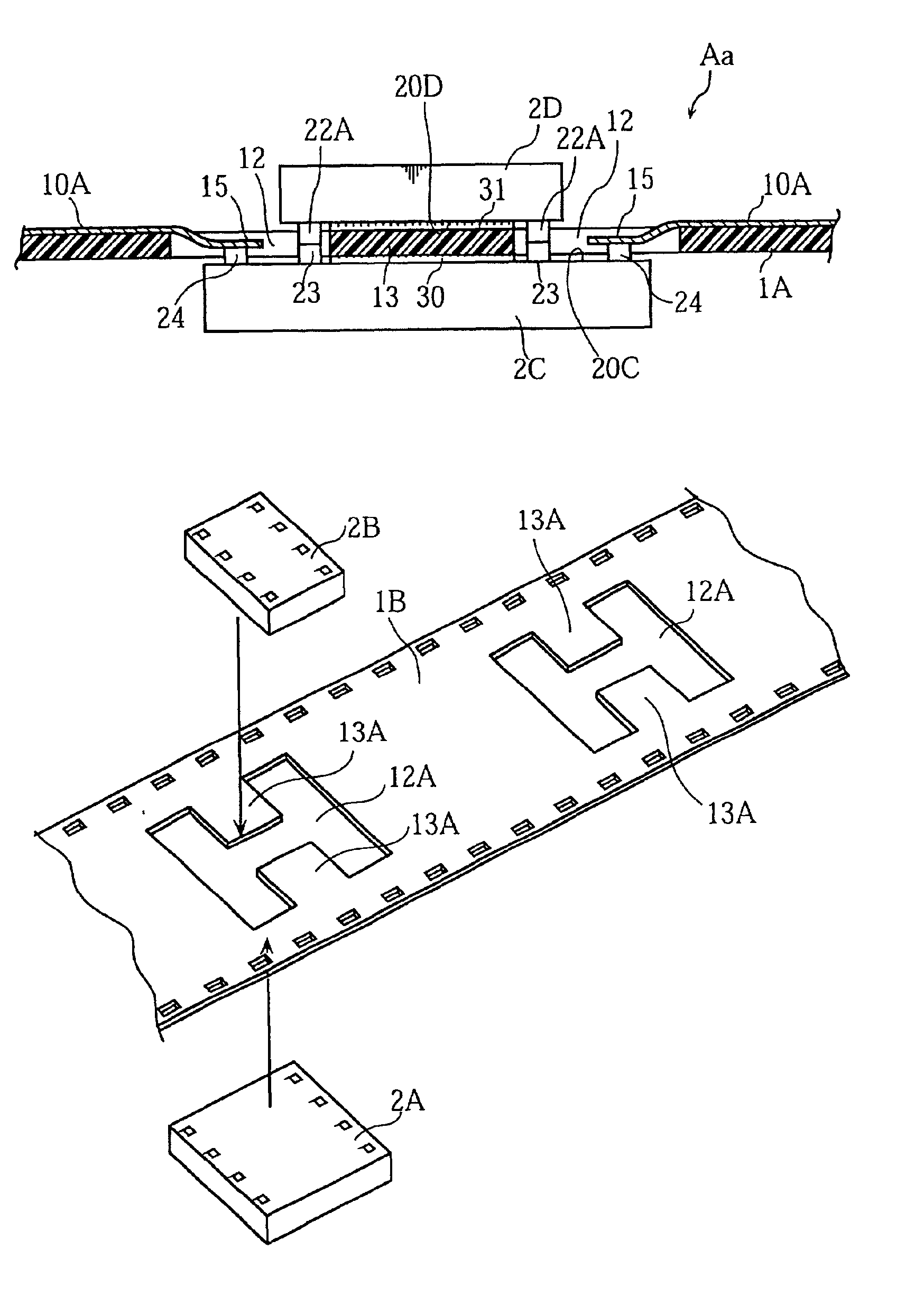
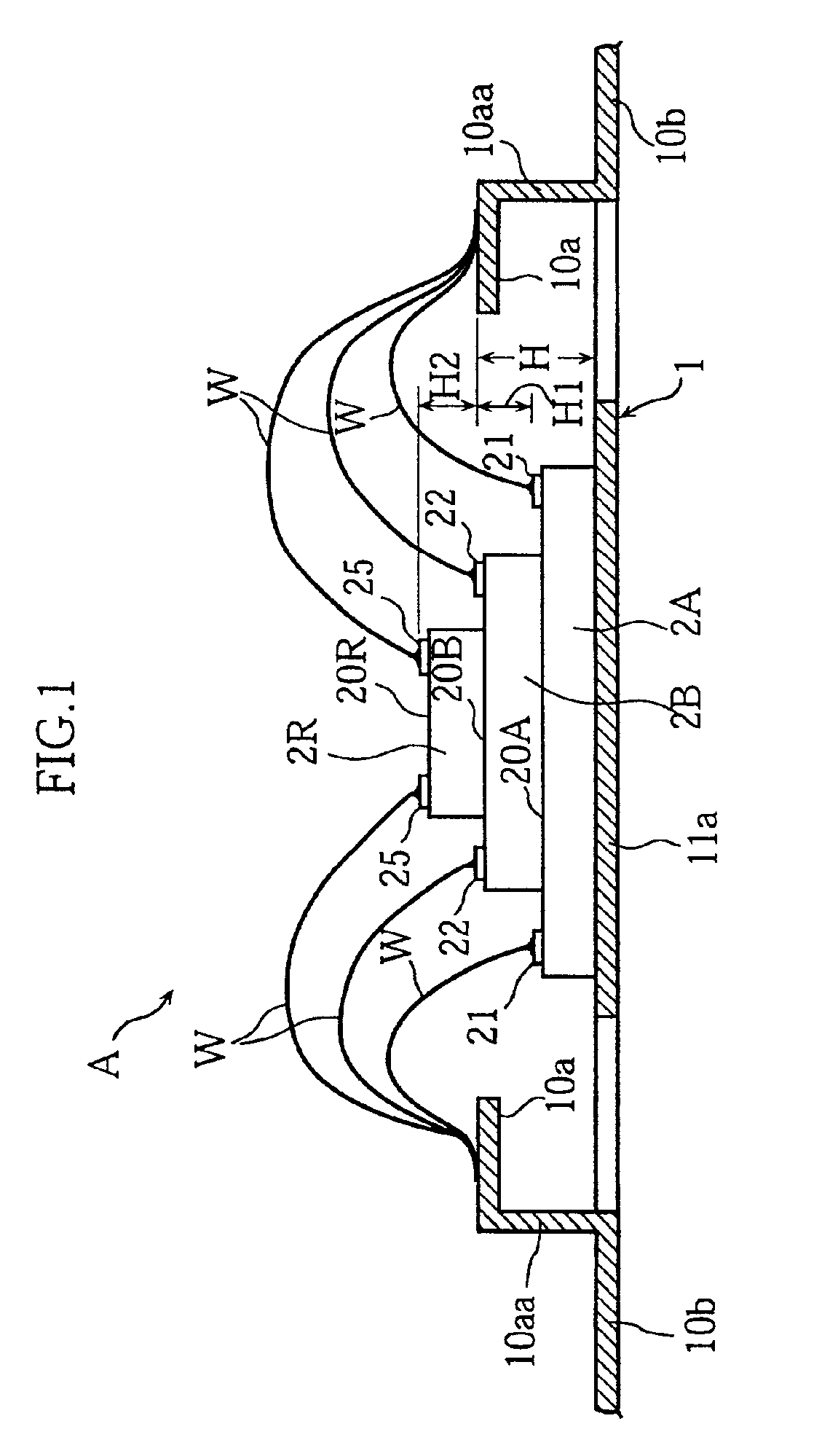
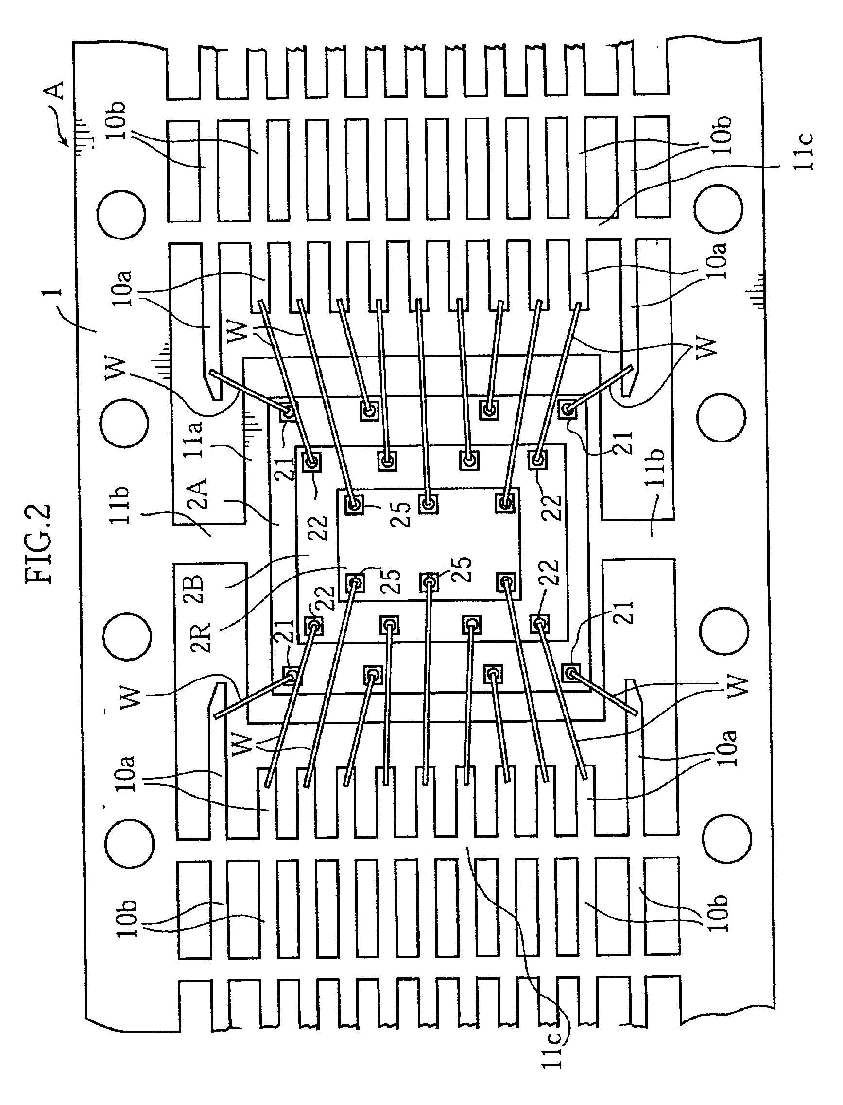
FIG. 1 is a sectional view showing a principal portion of an intermediate product A of a semiconductor device according to the present invention. FIG. 2 is a plan view of FIG. 1. The intermediate product A shown in these FIGS. 1 and 2 has an arrangement in which three semiconductor chips 2A, 2B, 2R are successively stacked one after another on a lead frame 1 in the direction of their thickness, and each of the three semiconductor chips 2A, 2B, 2R is connected to respective inner lead portions 10a of the lead frame 1 via a plural pieces of wire W. For convenience, the lowermost semiconductor chip 2A of the three semiconductor chips 2A, 2B, 2R will be called the first semiconductor chip herein. Likewise, the intermediate semiconductor chip 2B will be called the sec...


PUM


Abstract

A semiconductor device comprises a plurality of semiconductor chips stacked in the direction of thickness. Each of the semiconductor chips includes an upper surface formed with electrodes. The semiconductor device further comprises a plurality of terminal portions disposed beside these semiconductor chips, and a plural pieces of wire for electrical connection from the electrodes to respective terminal portions. Each of the terminal portions is at an elevation lower than the highest electrodes, and higher than the lowest electrodes.

Description

BACKGROUND OF THE INVENTION1. Field of the InventionThe present invention relates to a semiconductor device comprising a plurality of semiconductor chips stacked in the direction of thickness, and a method for making the same.2. Background ArtThere is known a type of semiconductor device in which a plurality of semiconductor chips are stacked and sealed in a resin package for drastically increased circuit mounting density. Such a semiconductor device is called “chip-on-chip” type because of the stacking arrangement in which one of the chips is mounted on another.FIG. 29 shows an arrangement of a prior art chip-on-chip semiconductor device. As understood from the figure, in this arrangement, a plurality of semiconductor chips 9a-9c are stacked successively on a surface of a substrate 90. According to such an arrangement, an area occupied by the semiconductor chips 9a-9c on the surface of substrate 90 is small, advantageously increasing the mounting density of the semiconductor device...

Claims


Application Information

Patent Timeline
Patent Type & Authority Patents(United States)
IPC IPC(8): H01L21/02H01L23/495H01L21/60H01L23/48H01L29/40
CPCH01L23/4951H01L24/32H01L24/49H01L24/50H01L24/85H01L24/91H01L24/97H01L23/49575H01L2224/32245H01L24/45H01L24/78H01L2224/0401H01L2224/05624H01L2224/05644H01L2224/16145H01L2224/32145H01L2224/32225H01L2224/45144H01L2224/4809H01L2224/48091H01L2224/48227H01L2224/4824H01L2224/48247H01L2224/4826H01L2224/48465H01L2224/4847H01L2224/48624H01L2224/49171H01L2224/4943H01L2224/73215H01L2224/73265H01L2224/78301H01L2224/78823H01L2224/85181H01L2224/92247H01L2224/97H01L2924/01002H01L2924/01005H01L2924/01007H01L2924/01013H01L2924/01014H01L2924/01029H01L2924/01056H01L2924/01057H01L2924/01074H01L2924/01075H01L2924/01079H01L2924/01082H01L2924/14H01L2924/15153H01L2924/15165H01L2924/15311H01L24/48H01L2924/01033H01L2924/014H01L2224/48644H01L2924/00014H01L2224/83H01L2224/85H01L2924/00H01L2924/00012H01L2924/10253H01L2924/07811H01L2224/06135H01L2924/15787H01L2924/181H01L2224/85205H01L2224/85207H01L2224/05554H01L24/73H01L2924/10161H01L24/86H01L2224/2612
Inventor OKA, HIROSHIHIROMITSU, MASAAKI
Owner ROHM CO LTD
Why Eureka
Try Eureka