Multi-chip stack flip-chip package

a technology of flip-chip packages and flip-chips, applied in the field of multi-chip stack flip-chip packages, can solve the problems of difficult to manufacture substrates with less than the pitch of bump pads, chip size becomes smaller and smaller, and the chip size is small and smaller

Active Publication Date: 2005-03-01
ADVANCED SEMICON ENG INC
View PDF7 Cites 80 Cited by
  • Summary
  • Abstract
  • Description
  • Claims
  • Application Information

AI Technical Summary

Benefits of technology

[0005]It is a first object of the present invention to provide a multi-chip stack flip-chip package including a dummy chip attached to a first flip chip on a substrate. The dummy chip has a redistribution layer (RDL) without active electrical function. A second flip chip is mounted on the dummy chip. The redistribution layer of the dummy chip electrically connects the second flip chip with the substrate skipping over the first flip chip to assemble a multi-chip package enabling the plurality of flip chips to be stacked repeatedly.

Problems solved by technology

However, the multi-chip flip-chip package can't achieve a vertical stack with the plurality of the flip chips.
In addition, the substrate is a well-known printed circuit board (PCB), the minimum pitch of bump pads of the PCB substrate is about 200 μm (micrometer) according to current PCB technology, it is difficult to manufacture the substrate with pitch of bump pads less than 150 μm by means of PCB process.
However the wiring pitch of the integrated circuits of the flip chip has reached 0.1 μm up-to-now which means that the chip size becomes smaller and smaller, and the bumps on the flip chip are more crowded.
Therefore, the yield of mass production of multi-chip flip-chip package cannot reach the acceptable range because it is not easy to make a substrate with bump pads in tiny pitch.
But it is very hard to design the C4 connection pads, bond pads and extra circuitry on the major surface of the integrated circuit chip.

Method used


Image

  • Multi-chip stack flip-chip package
  • Multi-chip stack flip-chip package
  • Multi-chip stack flip-chip package

Examples


second embodiment

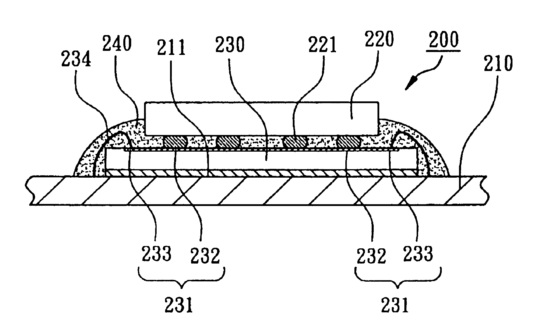
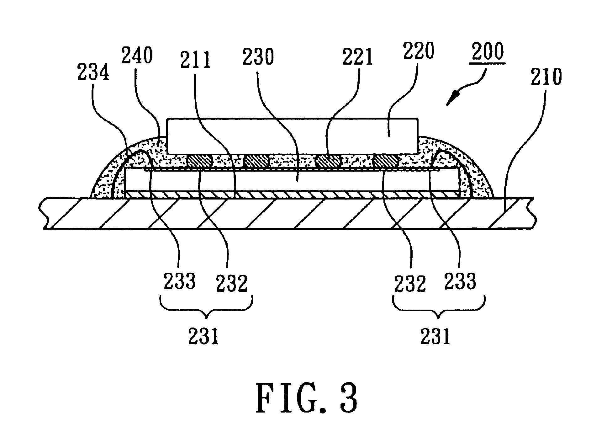
[0010]FIG. 3 is a cross-sectional view of the multi-chip stack flip-chip package in accordance with the present invention.

DETAILED DESCRIPTION OF THE PRESENT INVENTION

first embodiment

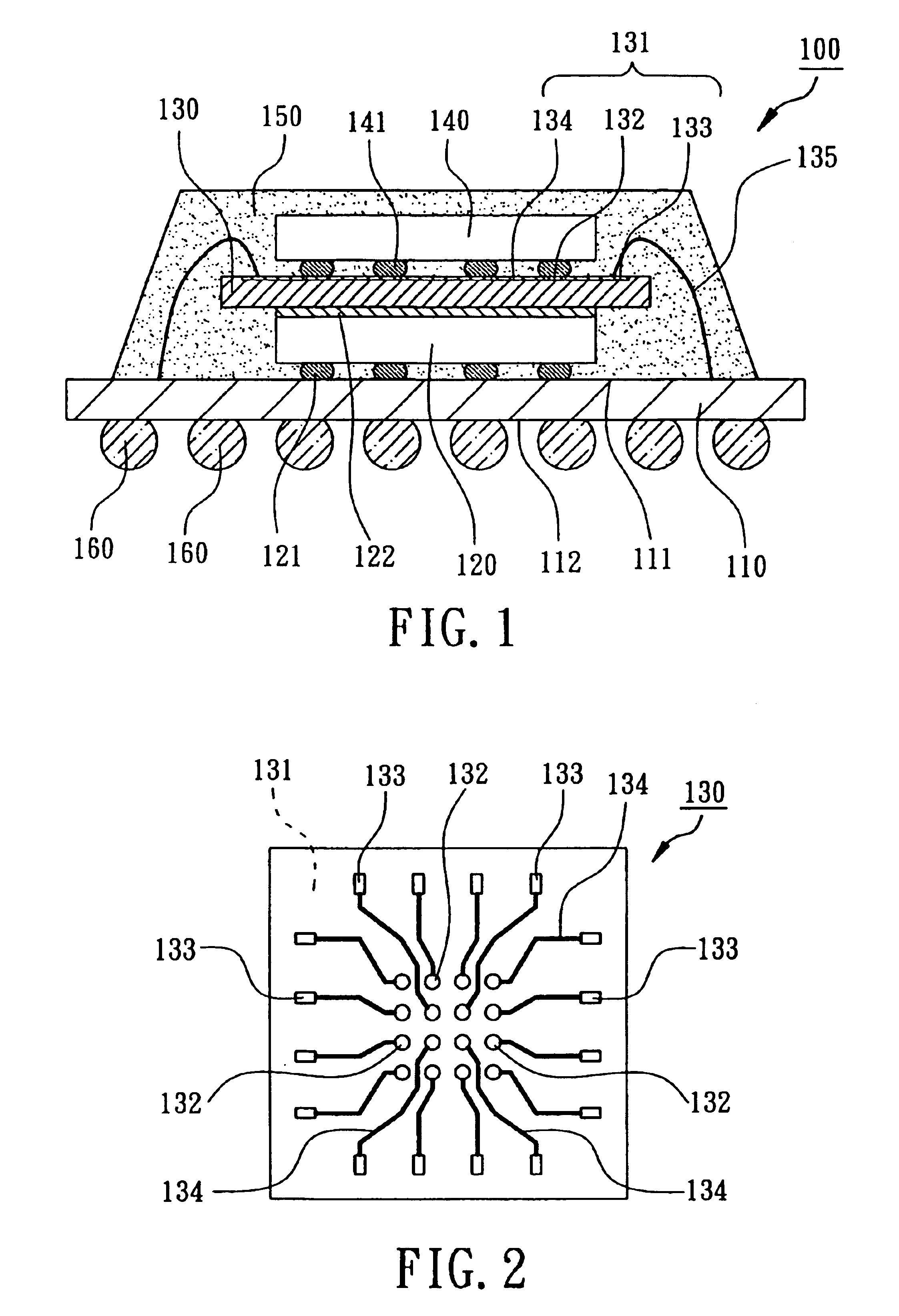
[0011]Referring to FIG. 1, a multi-chip stack flip-chip package 100 in accordance with the present invention comprises a substrate 110, at least a first flip chip 120, a dummy chip 130 and at least a second flip chip 140. The substrate 110 is a printed circuit board (PCB) formed by metal foil and glass fiber reinforced resin including BT resin, FR-4 resin or FR-5 resin. The substrate 110 has a top surface 111 and a bottom surface 112.

[0012]The first flip chip 120 is a chip with active electrical function, such as micro processor, micro controller, memory or Application Specific Integrated Circuit (ASIC). The first flip chip 120 has an active surface and a corresponding back surface. The first flip chip 120 includes a plurality of bumps 121 on its active surface. The first flip chip 120 is disposed on the top surface 111 of the substrate 110 by flip-chip mounting. Alternatively, the first flip chip 120 can be mounted on another dummy chip or a wire-bonding chip on the substrate 110 (...


PUM


Abstract

A multi-chip stack flip-chip package comprises a substrate and a chip assembly on the substrate. The chip assembly includes a dummy chip and a flip chip. The dummy chip has a redistribution layer that has a plurality of bump pads for mounting the flip chip, a plurality of peripheral pads for electrically connecting to the substrate, and a plurality of integrated circuit traces connecting the bump pads with the peripheral pads. The dummy chip is disposed between the flip chip and the substrate as an electrically connecting interface between the flip chip and the substrate for multi-chip flip-chip stack and fine pitch flip-chip mounting.

Description

FIELD OF THE INVENTION[0002]The present invention is generally relating to a multi-chip package (MCP), particularly to a multi-chip stack flip-chip package.BACKGROUND OF THE INVENTION[0003]It is well known that a multi-chip flip-chip package includes a plurality of flip chips with the bumps and a substrate for directly flip-chip mounting. In U.S. Pat. No. 6,507,098, Lo et al. disclosed a structure of a multi-chip stack package, which comprises a plurality of flip chips mounted on one surface of substrate. Each flip chip has a plurality of bumps on an active surface thereof for flip-chip (C4) mounting on the same surface of the substrate. The substrate is demanded to supply a large enough area for mounting the flip chips. However, the multi-chip flip-chip package can't achieve a vertical stack with the plurality of the flip chips. In addition, the substrate is a well-known printed circuit board (PCB), the minimum pitch of bump pads of the PCB substrate is about 200 μm (micrometer) ac...

Claims


Application Information

Patent Timeline
Patent Type & Authority Patents(United States)
IPC IPC(8): H01L25/065H01L23/31H01L23/28
CPCH01L23/3128H01L25/0657H01L2224/32225H01L2225/0651H01L2225/06517H01L2225/06527H01L2225/06582H01L2924/1433H01L2924/15311H01L2924/01087H01L2224/16225H01L2924/19107H01L2224/73253H01L2224/73204H01L2924/00012H01L2924/00
Inventor YANG, CHAUR-CHINWANG, SUNG-FEI
Owner ADVANCED SEMICON ENG INC
Why Eureka
Try Eureka