
Data access method of semiconductor memory device and semiconductor memory device

a data access and semiconductor technology, applied in the direction of information storage, static storage, digital storage, etc., can solve the problems of inability to increase the occupation rate of data bus data, the inability to achieve high speed access time “tce”, and the inability to occupy data bus data at the same time. , to achieve the effect of increasing the occupation rate of external access operation, reducing the differential amplification time in the refresh operation, and improving the efficiency

Inactive Publication Date: 2005-03-01
FUJITSU LTD
View PDF14 Cites 10 Cited by
  • Summary
  • Abstract
  • Description
  • Claims
  • Application Information

AI Technical Summary

Benefits of technology

The present invention provides a data access method for a semiconductor memory device that can effectively arrange a refresh operation within an external access operation, or between successive external access operations. This is achieved by making the differential amplification time of the bit line pair during the refresh operation shorter than the differential amplification time during the external access operation. This allows for a proper application of the refresh operation and improves the data-occupation rate in the data bus when a system is constituted. The data access method can be embedded in a semiconductor memory device that requires a new high-speed access operation specification or a semiconductor memory device that requires a high data-occupation rate specification.

Problems solved by technology

Therefore, there is such a problem that the access time “tCE” cannot be achived in a high speed.
Also, due to a similar reason, the cycle time “tCE” cannot be shortened.
Because of these difficulties, when a system is constituted, there are such problems that both a data-occupation rate and a data-transfer rate in a data bus cannot be increased.
As a result, the cycle time “tCE” cannot be shortened.
In the case that a system is constituted, there is another problem that both a data-occupation rate and a data-transfer rate in a data bus cannot be increased.
Also, as to the read operation among the external access operations, since the longer time (namely, tWT-tRD) than, or equal to the ability value is required for the amplification time “tRD”, this fact impedes shortening of both the access time and the cycle time in a similar manner.
When a system is constituted, both a data-occupation rate and a data-transfer rate in a data bus cannot be increased, resulting in another problem.

Method used


Image

  • Data access method of semiconductor memory device and semiconductor memory device
  • Data access method of semiconductor memory device and semiconductor memory device
  • Data access method of semiconductor memory device and semiconductor memory device

Examples


third embodiment

ng to the present invention;

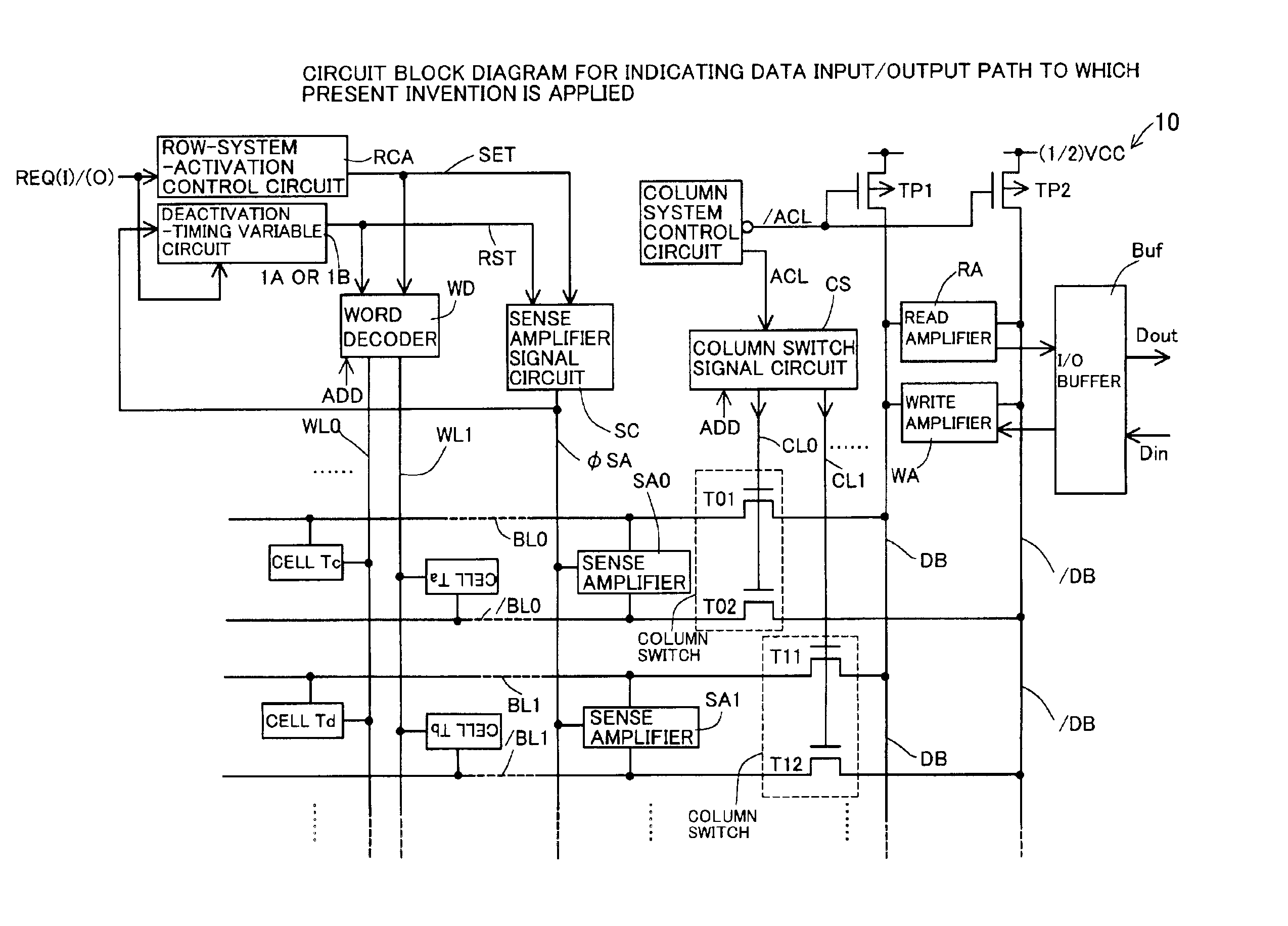
[0056]FIG. 9 is a circuit diagram for indicating a specific example of the third embodiment;

[0057]FIG. 10 is a timing chart for indicating operations of a burst length (1) in a synchronous type semiconductor memory device;

[0058]FIG. 11 is a timing chart for showing such a case that a refresh operation is embedded in the operations of the burst length (1) (fourth embodiment);

[0059]FIG. 12 is a timing chart for indicating operations of multiple burst length (8) in a synchronous type semiconductor memory device;

[0060]FIG. 13 is a timing chart for showing such a case that a refresh operation is embedded in the operations of the multiple burst length (8) (fifth embodiment);

[0061]FIG. 14 is a timing chart for indicating the external control refresh operation of the prior art;

[0062]FIG. 15 is a waveform diagram for representing the extension of the cycle time in the refresh operation of the prior art;

[0063]FIG. 16 is a timing chart for showing the refresh operat...


PUM


Abstract

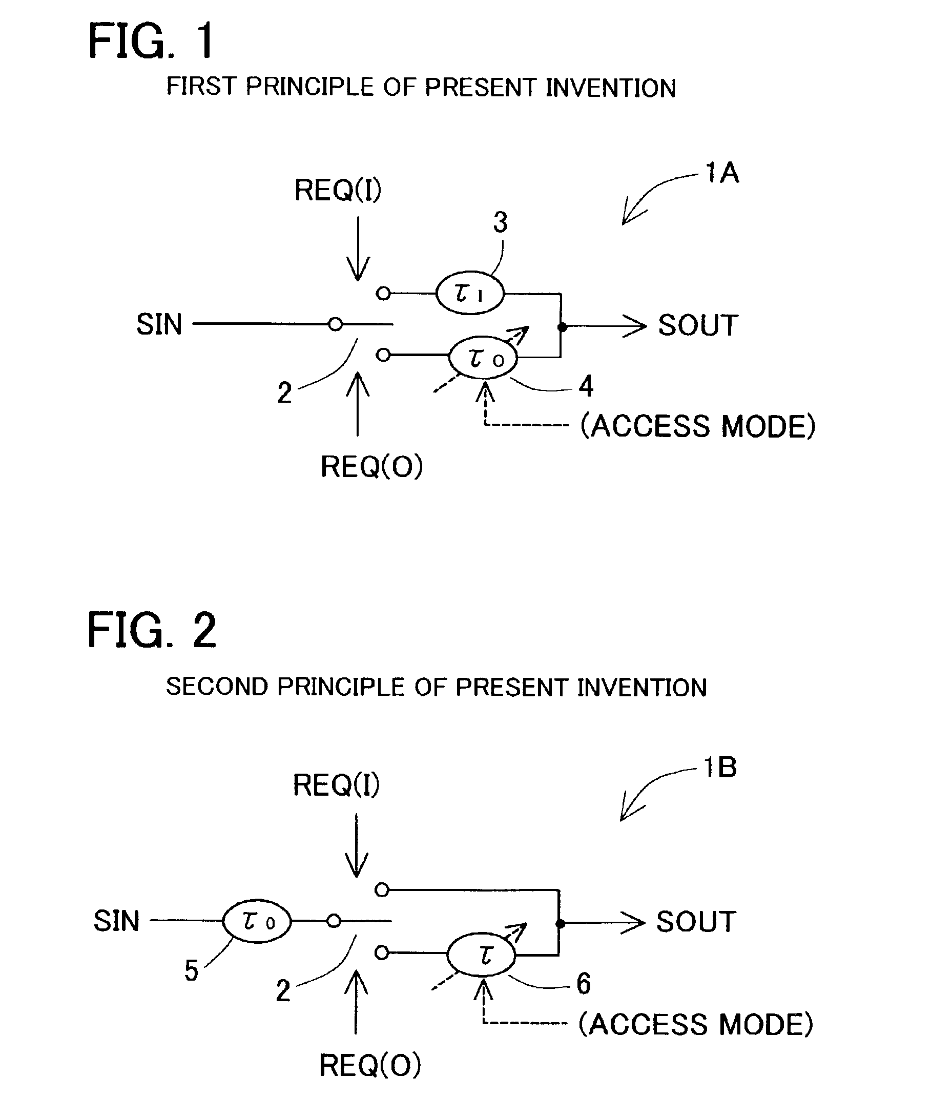
In the case that a refresh operation is carried out which is independent from an external access operation, both a data access method of a semiconductor memory device, and a semiconductor memory device are provided by which time suitable of each of these external access operation and refresh operation is set. While a time-measuring start signal “SIN” is entered into a path switching means, the path switching means is connected to either a first timer section or a second timer section under control of an external-access-operation-start-request signal REQ(O) and a refresh-operation-start-request signal REQ(I). Both the first and second timer sections measure both time “τO” and time “τI” to output a time-measuring stop signal “SOUT.” The measuring time “τO” corresponds to differential amplification time of a bit line pair when the external access operation is carried out, whereas the measuring time “τI” corresponds to differential amplification time when the refresh operation is carried out. Alternatively, the measuring time “τO” may be varied by reading / writing operations so as to be set. As a consequence, proper amplification time can be set every operation mode.

Description

BACKGROUND OF THE INVENTION[0002]1. Field of the Invention[0003]The present invention is generally related to a data access method of a semiconductor memory device in the case that a refresh operation is executed as an internal access operation which is independently carried out with respect to an external access operation, and also related to a semiconductor memory device. More specifically, the present invention is directed to a data access method of a semiconductor memory device, capable of effectively executing a refresh operation during an external access operation, or between successive external access operations, and also directed to a semiconductor device.[0004]2. Description of Related Art[0005]In volatile semiconductor memory devices which are typically known as dynamic random access memories (will be referred to as “DRAMs” hereinafter), refresh operations must be regularly carried out in order to maintain data stored in memory cells.[0006]FIG. 14 indicates operating wavef...

Claims


Application Information

Patent Timeline
Patent Type & Authority Patents(United States)
IPC IPC(8): G11C11/4076G11C11/406G11C11/407G11C7/08G11C11/403
CPCG11C11/4076G11C11/406G11C11/403
Inventor KATO, YOSHIHARU
Owner FUJITSU LTD
Learn More