Tunable microwave devices with auto-adjusting matching circuit

a matching circuit and microwave technology, applied in the field of tunable microwave devices, can solve the problems of impedance matching, impedance matching, and character impedance of the tunable components in the tunable microwave device not being constant values, so as to reduce reflections and reduce signal reflections

Inactive Publication Date: 2005-03-08
NXP USA INC
View PDF26 Cites 150 Cited by
  • Summary
  • Abstract
  • Description
  • Claims
  • Application Information

AI Technical Summary

Benefits of technology

The matching circuits form tunable impedance transformers that are able to match a constant microwave source impedance connected at the input port to a varying load impedance connected at the output port, thereby reducing signal reflections between the microwave source and a variable load impedance.
This invention provides an impedance matching circuit capable of matching a range of impedance values to a tunable microwave device in order to reduce reflections from impedance mismatch during tuning of the microwave device.

Problems solved by technology

However, the characteristic impedance of the tunable components in tunable microwave devices is not a constant value.
However, as the tunable microwave device is operated, the impedance of the tunable component varies from the matched impedance and a degradation in the impedance match occurs.
The disadvantage of the above technique is that the impedance match is optimal at one selective tuning point of the device and degrades as the device is tuned through its range.
Hence, the reflection loss due to impedance match increases when the device is tuned away from the matched point.
Since it is also desirable to reduce the insertion loss of the matching network, a disadvantage of the above approach is that the quarter wavelength transformer on tunable dielectric material increases the insertion loss.

Method used


Image

  • Tunable microwave devices with auto-adjusting matching circuit
  • Tunable microwave devices with auto-adjusting matching circuit
  • Tunable microwave devices with auto-adjusting matching circuit

Examples


first embodiment

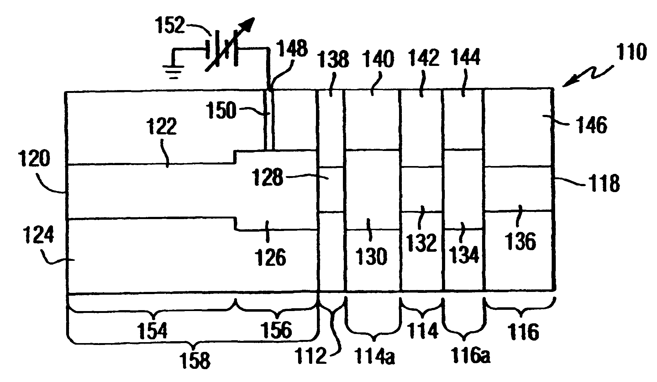
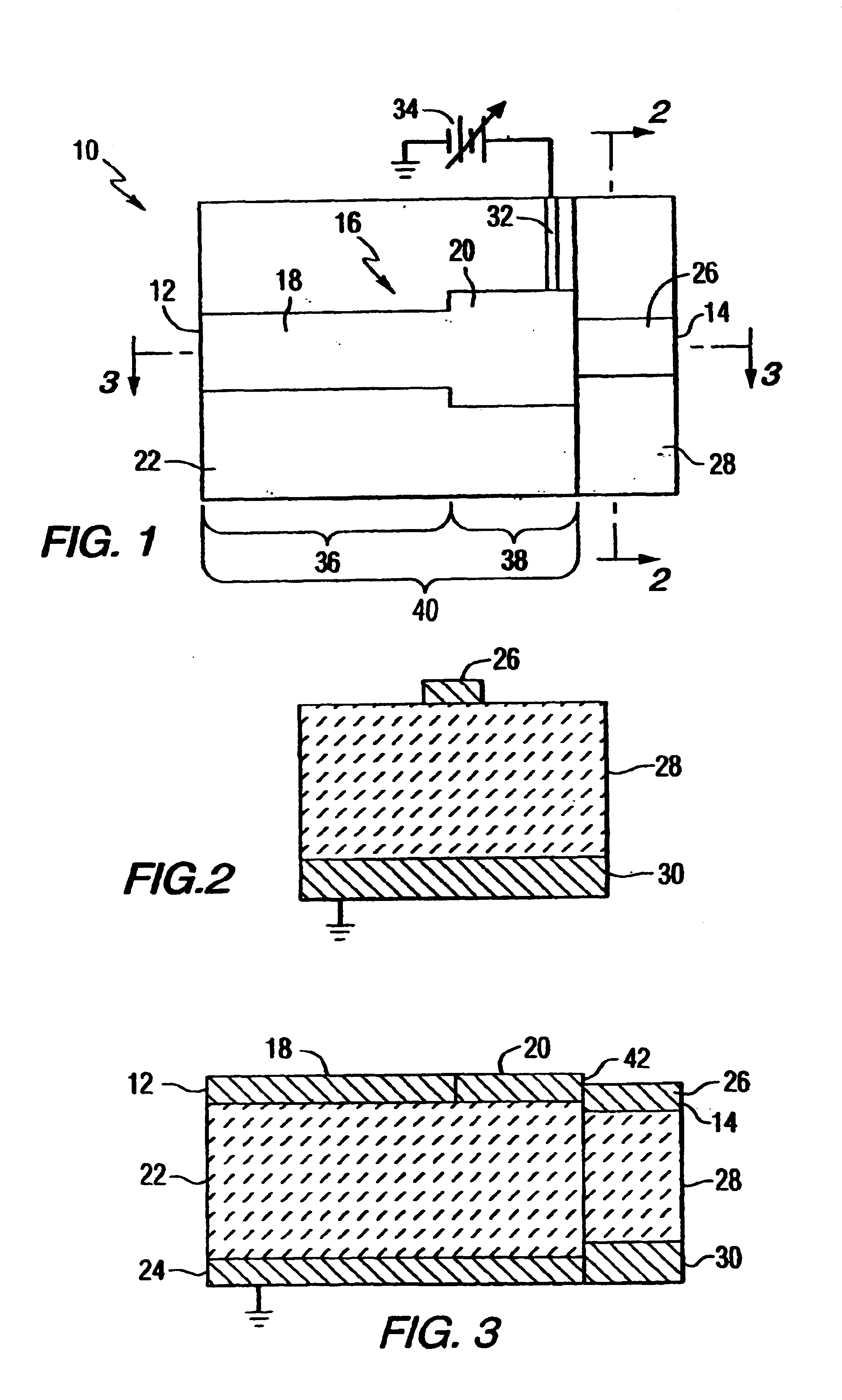
Referring to the drawings, FIG. 1 is a plan view of an auto adjusting matching network of this invention in the form of the microstrip circuit 10. FIG. 2 is a cross-sectional view of FIG. 1 taken along line 2—2, showing the microstrip line geometry. FIG. 3 is a cross-sectional view of FIG. 1 taken along line 3—3.

The device has two ports 12 and 14 for input and output of a guided electromagnetic wave. It includes a multi-stage microstrip line 16, having sections 18 and 20 of various widths and lengths, deposited on a non-tunable dielectric substrate22, which in turn is supported by ground plane 24; and a microstrip line section 26 deposited on a voltage tunable dielectric substrate 28 which in turn is supported by ground plane 30. A biasing electrode 32 in the form of a high impedance microstrip line is connected to microstrip section 20.

The biasing electrode 32 serves as a means for connecting an external variable DC bias voltage supply 34 to the auto-adjusting impedance matching ci...

second embodiment

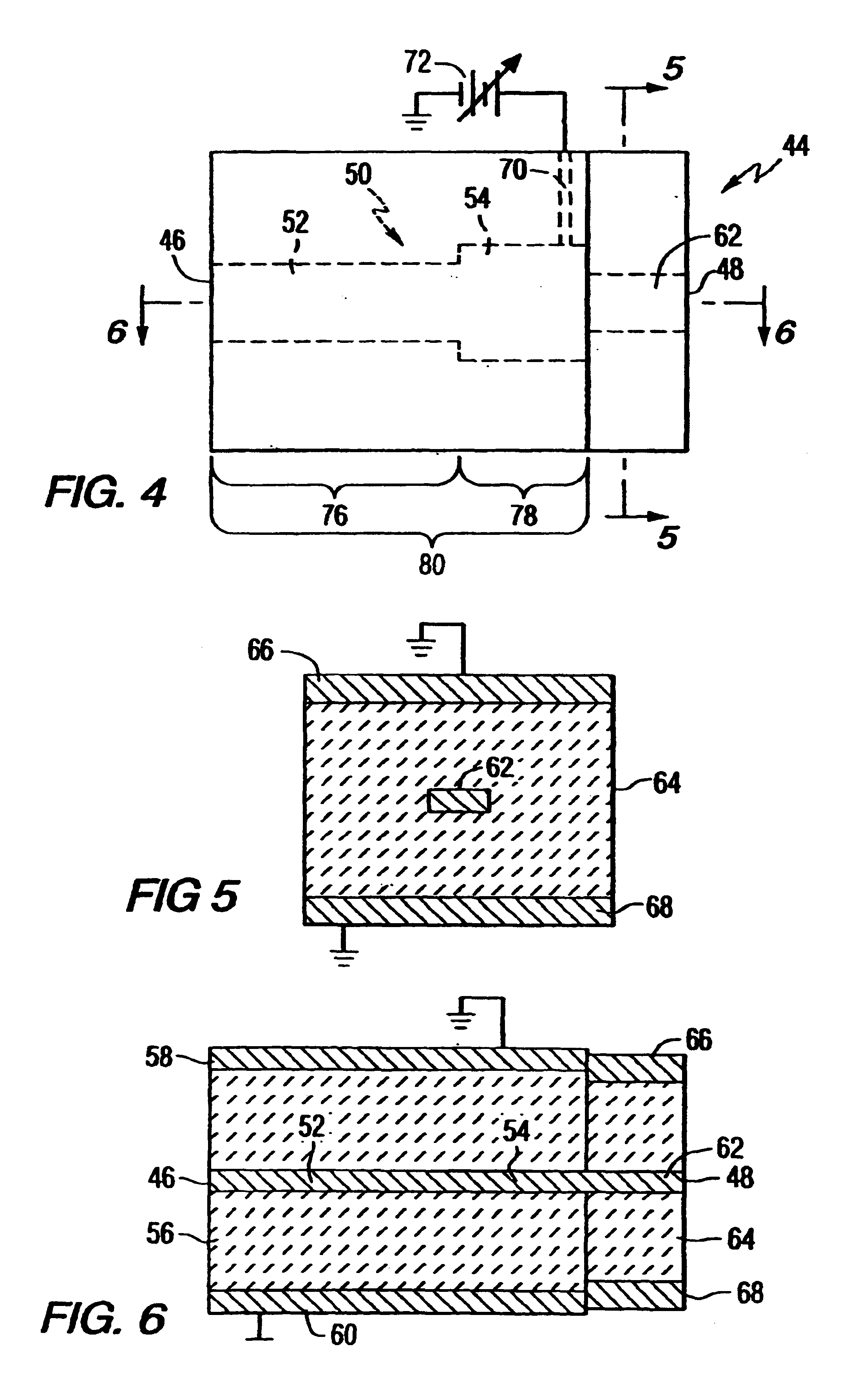
FIG. 4 is a plan view of the auto adjusting matching network 44 of the invention in the form of a stripline. FIG. 5 is a cross-sectional view of FIG. 4 taken along line 5—5, showing a stripline geometry. FIG. 6 is a cross-sectional view of FIG. 4 taken along line 6—6.

The device 44 has two ports 46 and 48 for input and output of the guided electromagnetic wave. It comprises a stripline 50 having sections 52 and 54 of various widths and lengths embedded in a non-tunable dielectric substrate 56 supported by top and bottom ground planes 58 and 60, an additional section 62 of stripline 50 embedded in a tunable dielectric substrate 64 supported by top and bottom ground planes 66 and 68, and a biasing electrode 70 in the form of a high impedance stripline is connected to stripline section 54.

The connection of biasing electrode 70 to the circuit is not limited to stripline section 54, but may be made to any other part of the circuit that is electrically connected to stripline section 62. Th...

third embodiment

FIG. 7 is a longitudinal cross-sectional view of the invention for the auto adjusting matching network based on a coaxial geometry. FIG. 8 is a cross-sectional view of FIG. 7 taken along line 8—8, showing the coaxial transmission line geometry.

The device 82 of FIGS. 7 and 8 has two ports 84 and 86 for input and output of the guided electromagnetic wave. It comprises a center conductor 88 having sections 90 and 92 of various diameters and lengths surrounded by a non-tunable dielectric substrate 94, which in turn is surrounded by ground conductor 96. An additional center conductor section 98 is surrounded by a tunable dielectric substrate 100, which in turn is surrounded by ground conductor 102. A thin biasing electrode 104 enters the co-axial structure through a small hole 106 and is connected to the central conductor 88.

The connection of biasing electrode 104 to the circuit is not limited to the center conductor section 92, but may be made to any other part of the circuit that is el...


PUM


Abstract

An impedance matching circuit includes a conductor line having an input port and an output port, a ground conductor, a tunable dielectric material positioned between a first section of the conductor line and the ground conductor, a non-tunable dielectric material positioned between a second section of the conductor line and the ground conductor, and means for applying a DC voltage between the conductor line and the ground conductor. The impedance matching circuit may alternatively include a first planar ground conductor, a second planar ground conductor, a strip conductor having an input port and an output port, and positioned between the first and second planar ground conductors to define first and second gaps, the first gap being positioned between the strip conductor and the first planar ground conductor and the second gap being positioned between the strip conductor and the second planar ground conductor. A non-tunable dielectric material supports the first and second planar ground conductors and the strip conductor in the same plane. A connection is provided for applying a DC voltage between the strip conductor and the first and second planar ground conductors. A plurality of tunable dielectric layer sections are positioned between the strip conductor and the first and second planar ground conductors so as to bridge the gaps between the said first and second planar ground conductors and the strip conductor at a plurality of locations, leaving non-bridged sections in between, defining a plurality of alternating bridged and non-bridged co-planar waveguide sections.

Description

FIELD OF THE INVENTIONThe invention relates to the field of tunable microwave devices. More specifically, the invention relates to impedance matching circuits that utilize a bias voltage to alter the permittivity of a tunable dielectric material.BACKGROUND OF THE INVENTIONMicrowave devices typically include a plurality of components that may have different characteristic impedances. In order to propagate the microwave signal through the device with minimal loss, the impedances of the various components are matched to the characteristic impedance of the input and output signal. By transitioning the impedances so that an input transmission line is matched, most of the available power from the input is delivered to the device. Historically, impedance matching techniques have treated the matching of components with constant characteristic impedances to a constant characteristic impedance of the input line, e.g. to 50 Ω. Multi-stage matching circuits have been utilized to obtain minimal ...

Claims


Application Information

Patent Timeline
Patent Type & Authority Patents(United States)
IPC IPC(8): H01P5/04
CPCH01P5/028H01P5/04H01Q1/242H04B1/0458H03F3/60H03H7/40H03F1/56
Inventor DU TOIT, CORNELIS FREDERIKRYAN, DEIRDRE A.
Owner NXP USA INC
Why Eureka
Try Eureka